SK4401
Quad Buffer/Receiver
HIGH-PERFORMANCE PRODUCTS
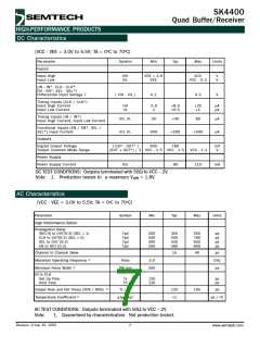
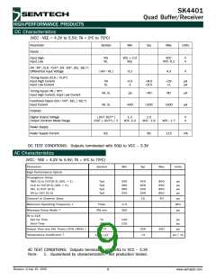
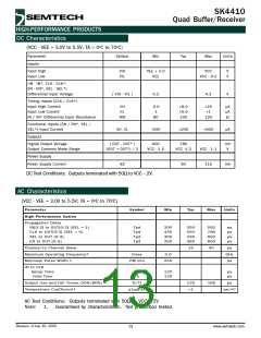
DC Characteristics
(VCC - VEE = 4.2V to 5.5V; TA = 0oC to 70oC)
Parameter
Inputs
Symbol
Min
Typ
Max
Units
Input High
Input Low
VIH
VIL
VEE + 2.0
VEE
VCC
VCC -0.2
V
V
(IN - IN*, CLK - CLK*, EN - EN*, SEL -SEL*)
Differential Input Voltage
| VIH - VIL |
0.2
4.3
V
Timing Inputs (CLK / CLK*)
Input High Current
Input Low Current
IIH
IIL
-5.0
-1
+8.0
<0.5
+25
+1
µA
µA
Timing Inputs (IN / IN*)
Input High Current, Input Low Current
IIH, IIL
IIH, IIL
<40
80
µA
µA
-20
Functional Inputs (EN / EN*, SEL / SEL*)
Input Current
-500
<200
+500
Outputs
Digital Output Voltage
Output Common Mode Range
| OUT -OUT* |
(OUT + OUT*) / 2
1.2
VCC -2.2
1.5
VCC - 1.9
V
V
VCC - 1.7
115
Power Supply
Power Supply Current
IEE
90
mA
DC TEST CONDITIONS: Outputs terminated with 50Ω to VCC – 3.3V
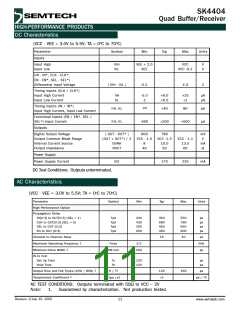
AC Characteristics
(VCC - VEE = 4.2V to 5.5V; TA = 0oC to 70oC)
Parameter
Symbol
Min
Typ
Max
Units
High Performance Option
Propagation Delay
IN[0:3] to OUT[0:3] (SEL = 1)
CLK to OUT[0:3] (SEL = 0)
SEL to OUT [0:3]
Tpd
Tpd
Tpd
Tpd
200
400
300
250
450
650
530
500
800
950
850
850
ps
ps
ps
ps
EN to OUT [0:3]
Channel to Channel Skew
15
40
ps
GHz
ps
1
Maximum Operating Frequency
Fmax
2.0
1
Minimum Pulse Width
PW min
350
IN to CLK
Set Up Time
Hold Time
Ts
Th
120
120
ps
ps
1
Output Rise and Fall Times (20% /80%)
Tr / Tf
200
<3
350
ps
1
o
Temperature Coefficient
ps /
C
∆Tpd /∆T
AC TEST CONDITIONS: Outputs terminated with 50Ω to VCC – 3.3V
Note: 1. Guaranteed by characterization. Not production tested.
Revision 1/July 10, 2002
9
www.semtech.com

 SEMTECH [ SEMTECH CORPORATION ]