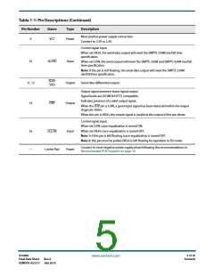
Table 1-1: Pin Descriptions (Continued)
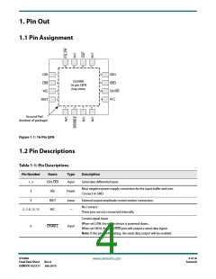
Pin Number
Name
Type
Description
Most positive power supply connection.
Connect to 3.3V or 2.5V.
9
VCC
Power
Control signal input.
When set HIGH, the serial data output will meet the SMPTE 259M rise/fall time
specification.
10
SD/HD
Input
When set LOW, the serial output will meet the SMPTE 292M and SMPTE 424M rise/fall
time specification.
Note: if this pin is left floating, the serial data output will meet the SMPTE 259M
rise/fall time specification.
SDO/
SDO
11, 12
14
Output
Output
Serial data differential output.
Output signal presence status signal output.
Signal levels are LVCMOS/LVTTL compatible.
Indicates presence of a valid output signal.
OSP
When the OSP pin is LOW, a good input signal has been detected within the output
stage pre-driver.
When this pin is HIGH, the output signal is invalid at the output of the pre-driver.
Control signal input.
When set LOW, trace-equalization is turned ON.
When set HIGH, trace-equalization is turned OFF.
Note 1: if this pin is left floating, trace-equalization is turned OFF.
Note 2: this pin must be pulled HIGH or left floating for operation in SD mode.
16
—
EQ_EN
Input
Connect to most negative power supply plane following the recommendations in
Recommended PCB Footprint on page 16.
Center Pad
Power
GS2988
Final Data Sheet
5 of 18
Semtech
www.semtech.com
Rev.6
GENDOC-052131 July 2015

 SEMTECH [ SEMTECH CORPORATION ]