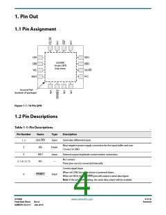
1. Pin Out
1.1 Pin Assignment
16
15
14
13
12
11
10
9
1
DDI
SDO
GS2988
16-pin QFN
(top view)
2
DDI
VEE
SDO
3
4
SD/HD
VCC
RSET
5
6
7
8
Ground Pad
(bottom of package)
Figure 1-1: 16-Pin QFN
1.2 Pin Descriptions
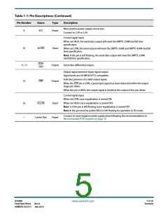
Table 1-1: Pin Descriptions
Pin Number
Name
Type
Description
1, 2
DDI, DDI
Input
Serial data differential input.
Most negative power supply connection for the input buffer and core.
Connect to GND.
3
VEE
RSET
N/C
Power
Input
—
4
External output amplitude control resistor connection.
No Connect.
5, 7, 8, 13, 15
These pins are not connected internally.
Control signal input.
When set LOW, the entire device is powered-down.
When set HIGH, the SDO/SDO pins will output a serial data signal.
Note: if this pin is left floating, the serial data output will be enabled.
6
DISABLE
Input
GS2988
Final Data Sheet
GENDOC-052131 July 2015
4 of 18
Semtech
www.semtech.com
Rev.6

 SEMTECH [ SEMTECH CORPORATION ]