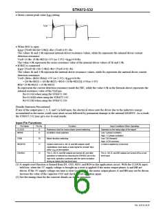
STK672-532
• Motor current peak value I
setting
OH
I
OH
0
• When RO2 is open
= [Vref×1k/(1k+3.9k)] ÷Rs= (Vref÷4.9) ÷Rs
I
OH
The values 1k and 3.9k represent internal driver resistance values, while Rs represents the internal driver current
detection resistance.
Vref= (4.9k÷ (4.9k+RO1)) ×5V (or 3.3V) =I ×4.9×Rs
OH
The value 4.9k represents the series resistance value of the internal driver values of 1k and 3.9k.
• If RO2 is connected
I
= [Vref×1k/ (1k+3.9k)] ÷Rs= (Vref÷4.9) ÷Rs
OH
The values 1k and 3.9k represent the internal driver resistance values, while Rs represents the internal driver current
detection resistance.
Vref= (R0x÷ (RO1+R0x)) ×5V (or 3.3V) =I ×4.9×Rs
OH
= [(4.9k×RO2) ÷ ((4.9k×RO2) +RO1× (4.9k+RO2))] ×5V(or 3.3V)
R0x= (4.9k×RO2) ÷ (4.9k+RO2)
Rs represents the current detection resistance inside the HIC, while the value 4.9k in the formula above represents the
internal resistance value of the Vref pin.
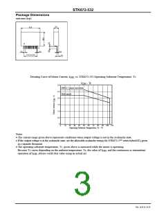
Rs=0.11Ω when using the STK672-540
Rs=0.165Ω when using the STK672-532
Rs=0.33Ω when using the STK672-520
[Smoke Emission Precuations]
If any of the output pins 2, 3, 4, and 5 is held open, the electrical stress onto the driver due to the inductive energy
accumulated in the motor could cause short-circuit followed by permanent damage to the internal MOSFET. As a result,
the STK672-532 may give rise to emit smoke.
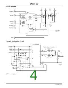
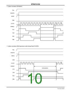
Input Pin Functions
Pin Name
Pin No.
Function
Reference clock for motor phase current switching
Excitation mode selection
Input Conditions When Operating
CLOCK
9
8
Operates on the rising edge of the signal
MODE
CWB
Low: 2-phase excitation
High: 1-2 phase excitation
Low: CW (forward)
10
11
Motor direction switching
High: CCW (reverse)
RESETB
System reset and A, AB, B, and BB outputs cutoff.
A reset is applied by a low level
Applications must apply a reset signal for at least 10μs
when V
is first applied.
DD
ENABLE
12
The A, AB, B, and BB outputs are turned off, and after
operation is restored by returning the ENABLE pin to the
high level, operation continues with the same excitation
timing as before the low-level input.
The A, AB, B, and BB outputs are turned off by a low-
level input.
(1) A simple reset function is formed from D1, CO2, RO3, and RO4 in this application circuit. With the CLOCK input
held low, when the 5V supply voltage is brought up a reset is applied if the motor output phases A and BB are
driven. If the 5V supply voltage rise time is slow (over 50ms), the motor output phases A and BB may not be driven.
Increase the value of the capacitor CO2 and check circuit operation again.
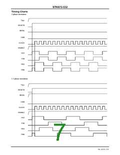
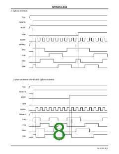
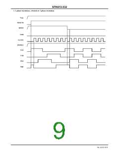
(2) See the timing chart for the concrete details on circuit operation.
No. A2111-6/23

 SANYO [ SANYO SEMICON DEVICE ]