STK672-532
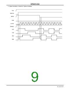
Specifications
Absolute Maximum Ratings at Tc = 25°C
Parameter
Maximum supply voltage 1
Maximum supply voltage 2
Input voltage
Symbol
max
Conditions
Ratings
unit
V
V
V
V
No signal
No signal
52
CC
max
-0.3 to +7.0
-0.3 to +7.0
5
V
DD
max
max
max
Logic input pins
V
IN
OP
OH
Output current 1
I
I
10μA 1 pulse (resistance load)
A
Output current 2
V
=5V, CLOCK≥200Hz
2.65
A
DD
Allowable power dissipation
Operating substrate temperature
Junction temperature
Storage temperature
Pd max
Tc max
Tj max
Tstg
With an arbitrarily large heat sink. Per MOSFET
10.2
W
°C
°C
°C
105
150
-40 to +125
Allowable Operating Ranges at Ta=25°C
Parameter
Operating supply voltage 1
Operating supply voltage 2
Input high voltage
Symbol
Conditions
Ratings
unit
V
V
V
V
V
With signals applied
With signals applied
Pins 8, 9, 10, 11, 12
Pins 8, 9, 10, 11, 12
10 to 42
5 5%
CC
V
DD
IH
IL
2.5 to V
V
DD
Input low voltage
0 to 0.6
V
Output current 1
I
1
Tc=105°C, CLOCK≥200Hz,
OH
2.0
A
Continuous operation, duty=100%
Output current 2
I
2
Tc=80°C, CLOCK≥200Hz,
OH
Continuous operation, duty=100%,
2.2
A
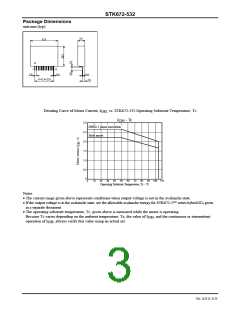
See the motor current (I
) derating curve
OH
CLOCK frequency
f
Minimum pulse width: at least 10μs
=1mA (Tc=25°C)
0 to 50
100min
kHz
V
CL
Phase driver withstand voltage
V
I
D
DSS
Recommended operating
substrate temperature
Tc
No condensation
0 to 105
°C
Recommended Vref range
Vref
Tc=105°C
0.14 to 1.62
V
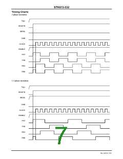
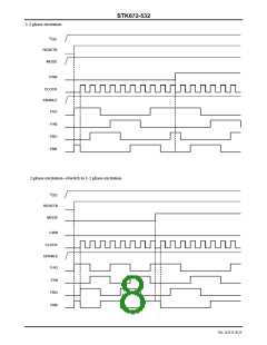
Refer to the graph for each conduction-period tolerance range for the output current and brake current.
Electrical Characteristics at Tc=25°C, V =24V, V =5.0V
CC
DD
Parameter
Symbol
Conditions
min
typ
max
unit
mA
A
V
supply current
I
Pin 6 current CLOCK=GND
3.1
7
DD
CCO
Output average current
FET diode forward voltage
Output saturation voltage
Input high voltage
Ioave
Vdf
R/L=3Ω/3.8mH in each phase
0.324
0.36
1.0
0.396
1.6
If=1A (R =23Ω)
V
L
Vsat
R =23Ω
0.45
0.64
V
L
V
Pins 8, 9, 10, 11, 12
Pins 8, 9, 10, 11, 12
Pins 8, 9, 10, 11, 12=GND and 5V
Pin 7 =1.0V
2.5
35
V
IH
Input low voltage
V
0.6
10
V
IL
Input leak current
I
μA
μA
kHz
IL
Vref input bias current
PWM frequency
I
204
45
216
55
IB
fc
Notes: A fixed-voltage power supply must be used.
No. A2111-2/23

 SANYO [ SANYO SEMICON DEVICE ]