LC866548/40/32/28/24A
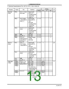
Pin Name
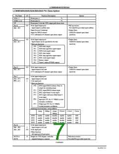
XT2/P75
I/O
O
Function Description
Option
•Output pin for 32.768kHz crystal oscillation
•Other function
P75 for input port
•In case of non use,
At using as oscillator, should be left opened.
At using as a port, connect to VDD1.
Input pin for ceramic resonator oscillation
Output pin for ceramic resonator oscillation
CF1
CF2
I
O
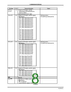
* All of port options (except pull-up resistor of port 0) can be specified in bit unit.
* A state of pins at reset
Pin name
Port 0
Input/output mode
Input
A state of pull-up resistor specified at pull-up option
Fixed pull-up resistor OFF
Ports 1, 3
Input
Programmable pull-up resistor OFF
S0/T0 to S15/T15
S16 to S51
P channel Transistor OFF
P channel Transistor OFF
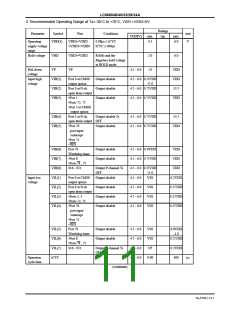
*1 Connect like the following figure to reduce noise into a VDD1 terminal.
• Shorted the VSS1 terminal to the VSS2 terminal and to make the back-up time long.
LSI
VDD1
Power
Back-up capacitor
VDD2
Supply
VDD3
VFD
powers
VDD4
VSS1
VSS2
No.6700-9/21

 SANYO [ SANYO SEMICON DEVICE ]