LC7930N, 7930NW
Continued from preceding page.
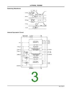
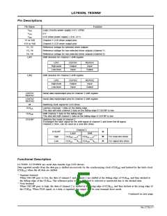
(1) Waveform Diagrams for Segment Drive Mode (CH2 – BP = ‘‘L’’)
(FLM)
M
CLKLA(latch)
CLKSR(shift)
Serial input data
Latch outputs
(Y1 to Y40)
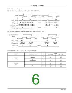
(2) Waveform Diagrams for Scan-Line/Segment Drive Mode (CH2–BP = ‘‘H’’)
LDATA2/RDATA2
(FLM)
M
CLKLA (shift)
CLKSR(latch)
Y21 to Y40
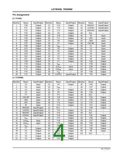
Table 1. LCD Driver Output Voltages (V1 to V6) for Y1 to Y40
Output
CH2–BP
Serial Input Data
M
Y1 to Y20
V1
Y21 to Y40
H
L
V2
V1
V6
V5
V1
V2
V5
V6
1
(selected)
V2
High level
(1)
H
L
V3
0
(un-selected)
V4
H
L
V1
1
0
V2
Low level
(2)
H
L
V3
V4
No.2778-6/7

 SANYO [ SANYO SEMICON DEVICE ]