LC7930N, 7930NW
Pin Descriptions
Pin Name
Function
V
Logic circuitry power supply (+5 V ±10%)
DD
V
0 V
SS
EE
V
LCD driver power supply (–4 to –6 V)
Channel 1 LCD driver output pins
Y1 to Y20
Y21 to Y40
V1, V2
Channel 2 LCD driver output pins
Reference voltage for selected driver outputs
Reference voltage for non-selected driver outputs (channel 1)
Reference voltage for non-selected driver outputs (channel 2)
Shift direction for channel 1 shift register
V3, V4
V5, V6
L/R1
L/R1
LDATA1
Output
Input
RDATA1
Input
High-level
Low-level
Output
L/R2
Shift direction for channel 2 shift register
L/R2
LDATA2
Output
Input
RDATA2
Input
High-level
Low-level
Output
LDATA1
RDATA1
Serial data input/output pins for channel 1 shift register
Serial data input/output pins for channel 2 shift register
Switching clock signal for LCD driver.
LDATA2
RDATA2
M
CLK
Latches channael 1 data on the falling edge.
This also will latch channel 2 data on the falling edge if CH2-BP is low.
LA
CLK
Shift channel 1 data on the falling edge.
This also will shift channel 2 data on the falling edge if CH2-BP is low.
SR
CH2-BP
Switches the mode of channel 2.
Exchanges the latch signal for the shift signal of channel 2 and invert the M signal.
Channel 2, then, can be used as a scan-line driver.
Channel 2
CH2-BP
M
Latch
SR
Shift
High
Low
CLK
CLK
CLK
CLK
M
M
For scan-line driver
For signal line driver
LA
SR
LA
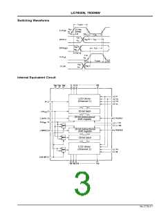
Functional Description
LC7930N, LC7930NW are serial data transfer type LCD drivers.
Data inputted serially from the data pin is shifted successively by the synchronizing clock (CLKSR) and latched by the latch clock
(CLKLA) when the all data are shifted.
.
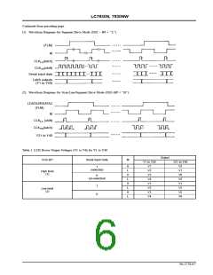
Segment terminal
When CH2-BP goes to low, the data of channel 1 and channel 2 are shifted at the falling edge of CLKSR, and then latched at
the falling edge of the CLKLA. The reference pulse will be switched to selected or unselected due to the latched data.
Scan terminal
When CH2-BP goes to high, the data of channel 2 is shifted at the rising edge of CLKLA, and then latched at the rising edge of
the CLKSR. When FLM signal, as a data, is inputted, the output will be scan terminal drive mode.
.
Continued on next page.
No.2778-5/7

 SANYO [ SANYO SEMICON DEVICE ]