LA4440
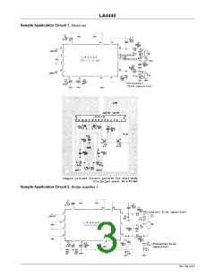
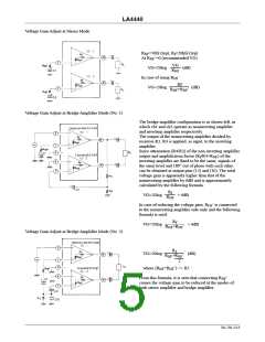
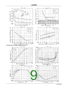
Sample Application Circuit 3. Bridge amplifier 2
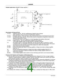
Description of External Parts
C1 (C2)
· Feedback capacitor : The low cutoff frequency depends on this capacitor.
If the capacitance value is increased, the starting time is delayed.
C3 (C4)
C5 (C6)
· Bootstrap capacitor : If the capacitance value is decreased, the output at low frequencies goes lower.
· Oscillation preventing capacitor : Polyester film capacitor, being good in temperature characteristic,
frequency characteristic, is used.
The capacitance value can be reduced to 0.047µF depending on the stability of the board.
· Output capacitor : The low cutoff frequency depends on this capacitor.
At the bridge amplifier mode, the output capacitor is generally connected.
· Decoupling capacitor :Used for the ripple filter. Since the rejection effect is saturated at a certain
capacitance value, it is meaningless to increase the capacitance value more than required. This capaci-
tor, being also used for the time constant of the muting circuit, affects the starting time.
· Filter resistor for preventing oscillation.
C7 (C8)
C9
R1 (R2)
R3 (R4)
· Resistor for making input signal of inverting amplifier in Voltage Gain Adjust at Bridge Amplifier
Mode (No. 1).
R5
C10
C11
· Resistor for adjusting starting time in Voltage Gain Adjust at Bridge Amplifier Mode (No. 2)
· Capacitor for preventing oscillation in Voltage Gain Adjust at Bridge Amplifier Mode (No. 2)
· Power source capacitor.
R6 (R7)
· Used at bridge amplifier mode in order to increase discharge speed and to secure transient stability.
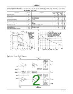
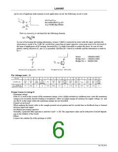
Feaures of IC System and Functions of Remaining Pins
(a) Since the input circuit uses PNP transistors and the input potential is designed to be 0 bias, no input coupling
capacitor is required and direct coupling is available. However, when slider contact noise caused by the variable
resistor presents a problem, connect an capacitor in series with the input.
(b) The open-loop voltage gain is lowered and the negative feedback amount is reduced for stabilization. An increase
in distortion resulted from the reduced negative feedback amount is avoided by use of the built-in unique distor-
tion reduction circuit, and thus distortion is kept at 0.1% (typ.).
(c) A capacitor for oscillation compensation is contained as a means of reducing the number of external parts. The
capacitance value is 35pF which determines high cutoff frequency f (–3dB point) of the amplifier (f ≈20kHz).
H
H
(d) For preventing the IC from being damaged by a surge applied on the power line, an overvoltage protector is
contained. Overvoltage setting is 25V. It is capable of withstanding up to 50V at giant pulse surge 200ms.
(e) No damege occurs even when power is applied at a state where pins 10, 11, and 12 are short-circuited with solder
bridge, etc.
(f) To minimize the variations in voltage gain, feedback resistor R is contained and voltage gain (51.5dB) is fixed.
NF
No.750–4/13

 SANYO [ SANYO SEMICON DEVICE ]