S3C70F2/C70F4/P70F4
S3P70F4 OTP
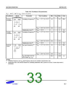
Table 16-6. Oscillators Characteristics
(TA = – 40 C + 85 C, VDD = 2.0 V to 5.5 V)
°
°
Oscillator
Clock
Parameter
Test Condition
Min Typ Max Units
Configuration
Oscillation frequency (1)
VDD = 2.7 V to 5.5 V
Ceramic
Oscillator
0.4
–
6.0
MHz
Xin
Xout
C1
C2
VDD = 2.0 V to 5.5 V
VDD = 3.0 V
0.4
–
–
–
–
4.2
4
Stabilization time (2)
ms
Oscillation frequency (1)
VDD = 2.7 V to 5.5 V
Crystal
Oscillator
0.4
6.0
MHz
Xin
Xout
C1
C2
VDD = 2.0 V to 5.5 V
VDD = 3.0 V
0.4
–
–
–
–
4.2
10
Stabilization time (2)
ms
X input frequency (1)
in
VDD = 2.7 V to 5.5 V
External
Clock
0.4
6.0
MHz
Xin
Xout
VDD = 2.0 V to 5.5 V
–
0.4
–
–
4.2
XIN input high and low
level width (tXH, tXL)
83.3
1250
ns
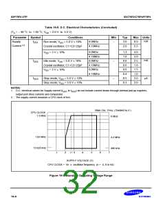
NOTES:
1. Oscillation frequency and X input frequency data are for oscillator characteristics only.
IN
2. Stabilization time is the interval required for oscillating stabilization after a power-on occurs, or when stop mode is
terminated.
16–7

 SAMSUNG [ SAMSUNG ]