S3C4510B
INSTRUCTION SET
OFFSETS AND AUTO-INDEXING
The offset from the base may be either a 12 bit unsigned binary immediate value in the instruction, or a second
register (possibly shifted in some way). The offset may be added to (U = 1) or subtracted from (U = 0) the base
register Rn. The offset modification may be performed either before (pre-indexed, P = 1) or after (post-indexed, P
= 0) the base is used as the transfer address.
The W bit gives optional auto increment and decrement addressing modes. The modified base value may be
written back into the base (W = 1), or the old base value may be kept (W = 0). In the case of post-indexed
addressing, the write back bit is redundant and is always set to zero, since the old base value can be retained by
setting the offset to zero. Therefore post-indexed data transfers always write back the modified base. The only
use of the W bit in a post-indexed data transfer is in privileged mode code, where setting the W bit forces non-
privileged mode for the transfer, allowing the operating system to generate a user address in a system where the
memory management hardware makes suitable use of this hardware.
SHIFTED REGISTER OFFSET
The 8 shift control bits are described in the data processing instructions section. However, the register specified
shift amounts are not available in this instruction class. See Figure 3-5.
BYTES AND WORDS
This instruction class may be used to transfer a byte (B = 1) or a word (B = 0) between an ARM7TDMI register
and memory.
The action of LDR(B) and STR(B) instructions is influenced by the BIGEND control signal of ARM7TDMI core.
The two possible configurations are described below.
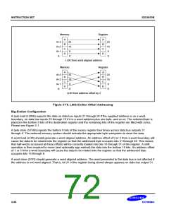
Little-Endian Configuration
A byte load (LDRB) expects the data on data bus inputs 7 through 0 if the supplied address is on a word
boundary, on data bus inputs 15 through 8 if it is a word address plus one byte, and so on. The selected byte is
placed in the bottom 8 bits of the destination register, and the remaining bits of the register are filled with zeros.
Please see Figure 2-2.
A byte store (STRB) repeats the bottom 8 bits of the source register four times across data bus outputs 31
through 0. The external memory system should activate the appropriate byte subsystem to store the data.
A word load (LDR) will normally use a word aligned address. However, an address offset from a word boundary
will cause the data to be rotated into the register so that the addressed byte occupies bits 0 to 7. This means that
half-words accessed at offsets 0 and 2 from the word boundary will be correctly loaded into bits 0 through 15 of
the register. Two shift operations are then required to clear or to sign extend the upper 16 bits.
A word store (STR) should generate a word aligned address. The word presented to the data bus is not affected if
the address is not word aligned. That is, bit 31 of the register being stored always appears on data bus output 31.
3-29

 SAMSUNG [ SAMSUNG ]