SYSTEM MANAGER
S3C4510B
DRAM INTERFACE FEATURES
The S3C4510B provides a fully programmable external DRAM interface. You can easily modify the
characteristics of this interface by manipulating the corresponding DRAM control registers. Programmable
features include
·
·
·
·
·
External data bus width
Control fast page or EDO mode by DRAMCON[0]
Select fast page/EDO mode or SDRAM mode by SYSCFG
Number of access cycles for each DRAM bank, and
CAS strobe time, CAS precharge time, RAS to CAS delay, RAS pre-charge time
The refresh and external I/O control register, REFEXTCON, controls DRAM refresh operations and external I/O
bank accesses. The S3C4510B eliminates the need for an external refresh signal by automatically issuing an
internal CAS-before-RAS refresh or auto-refresh control signal.
The S3C4510B generates row and column addresses for DRAM accesses with 23-bit internal address bus. It also
supports symmetric or asymmetric DRAM addressing by changing the number of column address lines from 8 to
11.
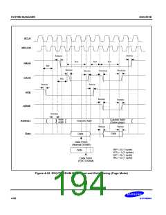
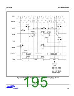
EDO Mode DRAM Accesses
The timing for accessing a DRAM in EDO mode is comparable to DRAM accesses in normal fast page mode.
However, in EDO mode, the S3C4510B CPU fetches data (when read) one-half clock later than in normal fast
page mode. This is possible because EDO mode can validate the data even if CAS goes High when RAS is Low.
In this way, gives the CPU sufficient time to access and latch the data so that the overall memory access cycle
time can be reduced.
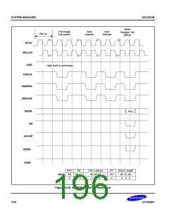
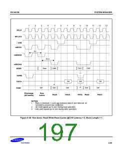
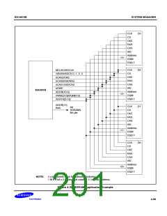
Synchronous DRAM Accesses
Synchronous DRAM interface features are as follows:
·
MRS cycle with address key program
— CAS latency (2 cycles)
— Burst length (1)
— Burst type (Sequential)
·
·
Auto refresh
SDRAM interface signal: CKE, SDCLK, nSDCS[3:0], nSDCAS, nSDRAS, DQM[3:0], ADDR[10]/AP
The address bits except row and column address among the 23-bit internal address bus can be assigned to Bank
select address(BA) for SDRAM.
See the SDRAM interface example, Figure 4-36.
4-56

 SAMSUNG [ SAMSUNG ]