S3C4510B
SYSTEM MANAGER
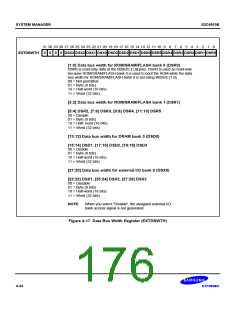
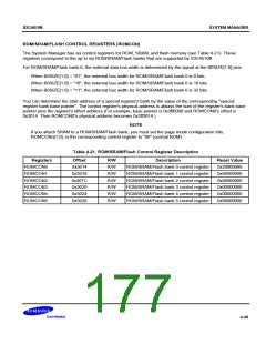
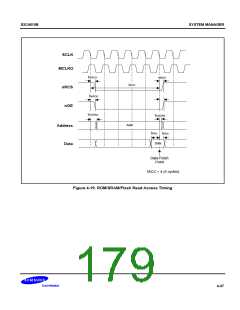
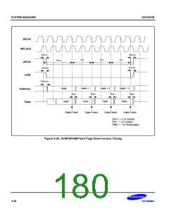
ROM/SRAM/FLASH CONTROL REGISTERS (ROMCON)
The System Manager has six control registers for ROM, SRAM, and flash memory (see Table 4-21). These
registers correspond to the up to six ROM/SRAM/Flash banks that are supported by S3C4510B.
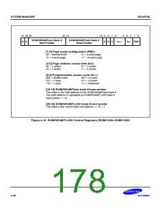
For ROM/SRAM/Flash bank 0, the external data bus width is determined by the signal at the B0SIZE[1:0] pins:
When B0SIZE[1:0] = "01", the external bus width for ROM/SRAM/Flash bank 0 is 8 bits.
When B0SIZE[1:0] = "10", the external bus width for ROM/SRAM/Flash bank 0 is 16 bits.
When B0SIZE[1:0] = "11", the external bus width for ROM/SRAM/Flash bank 0 is 32 bits.
You can determine the start address of a special register's bank by the value of the corresponding "special
register bank base pointer". The control register's physical address is always the sum of the register's bank base
pointer plus the register's offset address.(For example, base pointer is 0x3ff0000 and ROMCON0’s offset is
0x3014. Then ROMCON0’s physical address becomes 0x3ff3014.)
NOTE
If you attach SRAM to a ROM/SRAM/Flash bank, you must set the page mode configuration bits,
ROMCONn[1:0], in the corresponding control register to "00" (normal ROM).
Table 4-21. ROM/SRAM/Flash Control Register Description
Registers
ROMCON0
ROMCON1
ROMCON2
ROMCON3
ROMCON4
ROMCON5
Offset
0x3014
0x3018
0x301C
0x3020
0x3024
0x3028
R/W
R/W
R/W
R/W
R/W
R/W
R/W
Description
Reset Value
0x20000060
0x00000060
0x00000060
0x00000060
0x00000060
0x00000060
ROM/SRAM/Flash bank 0 control register
ROM/SRAM/Flash bank 1 control register
ROM/SRAM/Flash bank 2 control register
ROM/SRAM/Flash bank 3 control register
ROM/SRAM/Flash bank 4 control register
ROM/SRAM/Flash bank 5 control register
4-35

 SAMSUNG [ SAMSUNG ]