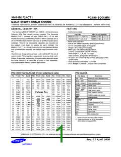
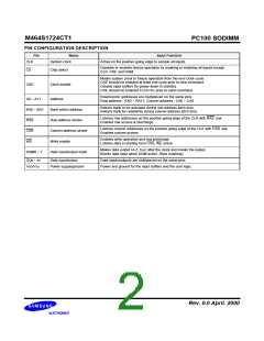
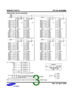
M464S1724CT1
PC100 SODIMM
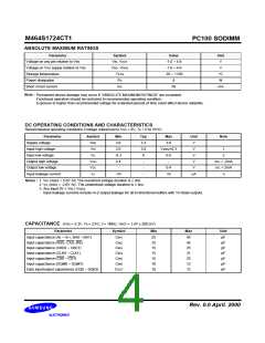
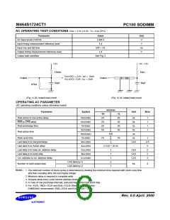
AC OPERATING TEST CONDITIONS (VDD = 3.3V ± 0.3V, TA = 0 to 70°C)
Parameter
AC input levels (Vih/Vil)
Value
2.4/0.4
1.4
Unit
V
Input timing measurement reference level
Input rise and fall time
V
tr/tf = 1/1
1.4
ns
V
Output timing measurement reference level
Output load condition
See Fig. 2
3.3V
Vtt = 1.4V
1200W
50W
VOH (DC) = 2.4V, IOH = -2mA
VOL (DC) = 0.4V, IOL = 2mA
Output
Output
Z0 = 50W
50pF
50pF
870W
(Fig. 1) DC output load circuit
(Fig. 2) AC output load circuit
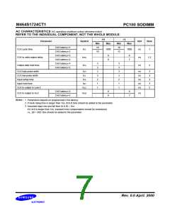
OPERATING AC PARAMETER
(AC operating conditions unless otherwise noted)
Version
Parameter
Symbol
Unit
Note
-1H
20
20
20
50
-1L
20
20
20
50
Row active to row active delay
RAS to CAS delay
tRRD(min)
tRCD(min)
tRP(min)
ns
ns
1
1
1
1
Row precharge time
ns
tRAS(min)
tRAS(max)
tRC(min)
ns
Row active time
100
2
us
Row cycle time
70
70
ns
1
2,5
5
Last data in to row precharge
Last data in to Active delay
Last data in to new col. address delay
Last data in to burst stop
tRDL(min)
tDAL(min)
tCDL(min)
tBDL(min)
tCCD(min)
CLK
-
2 CLK + 20 ns
1
1
1
2
1
CLK
CLK
CLK
2
2
Col. address to col. address delay
3
CAS latency=3
CAS latency=2
Number of valid output data
ea
4
Notes :
1. The minimum number of clock cycles is determined by dividing the minimum time required with clock cycle time
and then rounding off to the next higher integer.
2. Minimum delay is required to complete write.
3. All parts allow every cycle column address change.
4. In case of row precharge interrupt, auto precharge and read burst stop.
5. For -1H/1L, tRDL=1CLK and tDAL=1CLK+20ns is also supported .
SAMSUNG recommends tRDL=2CLK and tDAL=2CLK + 20ns.
Rev. 0.0 April. 2000

 SAMSUNG [ SAMSUNG ]