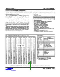
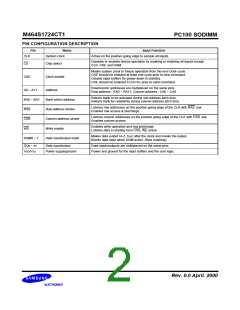
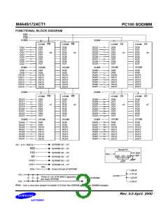
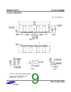
M464S1724CT1
PC100 SODIMM
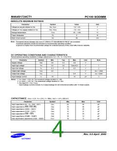
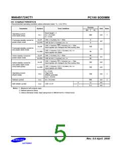
ABSOLUTE MAXIMUM RATINGS
Parameter
Voltage on any pin relative to Vss
Voltage on VDD supply relative to Vss
Storage temperature
Symbol
VIN, VOUT
VDD, VDDQ
TSTG
Value
-1.0 ~ 4.6
-1.0 ~ 4.6
-55 ~ +150
8
Unit
V
V
°C
W
Power dissipation
PD
Short circuit current
IOS
50
mA
Note :
Permanent device damage may occur if "ABSOLUTE MAXIMUM RATINGS" are exceeded.
Functional operation should be restricted to recommended operating condition.
Exposure to higher than recommended voltage for extended periods of time could affect device reliability.
DC OPERATING CONDITIONS AND CHARACTERISTICS
Recommended operating conditions (Voltage referenced to VSS = 0V, TA = 0 to 70°C)
Parameter
Supply voltage
Symbol
VDD
VIH
Min
3.0
2.0
-0.3
2.4
-
Typ
Max
Unit
V
Note
3.3
3.6
Input high voltage
Input low voltage
3.0
VDDQ+0.3
V
1
VIL
0
-
0.8
-
V
2
Output high voltage
Output low voltage
Input leakage current
VOH
VOL
ILI
V
IOH = -2mA
IOL = 2mA
3
-
0.4
10
V
-10
-
uA
Notes :
1. VIH (max) = 5.6V AC.The overshoot voltage duration is £ 3ns.
2. VIL (min) = -2.0V AC. The undershoot voltage duration is £ 3ns.
3. Any input 0V £ VIN £ VDDQ.
Input leakage currents include Hi-Z output leakage for all bi-directional buffers with Tri-State outputs.
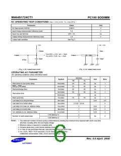
CAPACITANCE (VDD = 3.3V, TA = 23°C, f = 1MHz, VREF = 1.4V ± 200 mV)
Parameter
Symbol
Min
Max
Unit
Input capacitance (A0 ~ A11, BA0 ~ BA1)
Input capacitance (RAS, CAS, WE)
Input capacitance (CKE0 ~ CKE1)
Input capacitance (CLK0 ~ CLK1)
Input capacitance (CS0 ~ CS1)
CIN1
CIN2
CIN3
CIN4
CIN5
CIN6
COUT
25
25
15
15
15
10
10
45
45
25
21
25
12
12
pF
pF
pF
pF
pF
pF
pF
Input capacitance (DQM0 ~ DQM7)
Data input/output capacitance (DQ0 ~ DQ63)
Rev. 0.0 April. 2000

 SAMSUNG [ SAMSUNG ]