OneNAND512Mb(KFG1216U2B-xIB6)
FLASH MEMORY
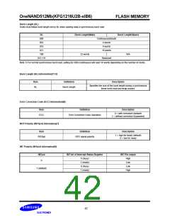
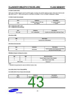
I/O Buffer Enable (IOBE)
IOBE is the I/O Buffer Enable for the INT and RDY signals. At startup, INT and RDY outputs are High-Z. Bits 6 and 7 become valid
after IOBE is set to "1". IOBE can be reset by a Cold Reset or by writing "0" to bit 5 of System Configuration1 Register.
I/O Buffer Enable Information[5]
Item
Definition
Description
I/O Buffer Enable for INT and
RDY signals
0 = disable (default)
1 = enable
IOBE
RDY Configuration (RDY conf)
RDY Configuration Information[4]
Item
Definition
Description
RDY conf
RDY configuration
0=active one clock before valid data (Fixed)
Write Mode (WM)
WM
Write Mode
Asynchronous Write(default)
0
Write Mode Information[1]
Item
Definition
Description
Selects between asynchronous Write Mode
and synchronousWrite Mode
WM
Write Mode
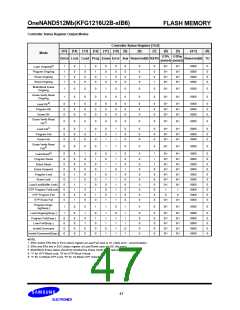
MRS(Mode Register Setting) Description
RM
0
WM
0
Mode Description
Asynch Read & Asynch Write (Default)
1
0
Sync Read & Asynch Write
Reserved 1)
Other Cases
Note)
1. Operation not guaranteed for cases not defined in above table.
Boot Buffer Write Protect Status(BWPS)
Boot Buffer Write Protect Status Information[0]
Item
Definition
Description
0=locked(fixed)
BWPS
Boot Buffer Write Protect Status
43

 SAMSUNG [ SAMSUNG ]