K9F5608U0B-VCB0,VIB0,FCB0,FIB0
K9F5608Q0B-DCB0,DIB0,HCB0,HIB0
K9F5608U0B-YCB0,YIB0,PCB0,PIB0
K9F5608U0B-DCB0,DIB0,HCB0,HIB0
K9F5616Q0B-DCB0,DIB0,HCB0,HIB0
K9F5616U0B-YCB0,YIB0,PCB0,PIB0
K9F5616U0B-DCB0,DIB0,HCB0,HIB0
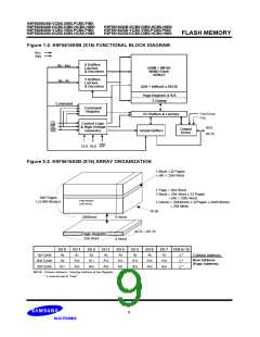
FLASH MEMORY
Document Title
32M x 8 Bit , 16M x 16 Bit NAND Flash Memory
Revision History
Revision No. History
Draft Date
Remark
0.5
1. Add the Rp vs tr ,tf & Rp vs ibusy graph for 1.8V device (Page 33)
Nov. 22.2002
2. Add the data protection Vcc guidence for 1.8V device - below about
1.1V. (Page 34)
0.6
0.7
The min. Vcc value 1.8V devices is changed.
K9F56XXQ0B : Vcc 1.65V~1.95V --> 1.70V~1.95V
Mar. 6.2003
Pb-free Package is added.
K9F5608U0B-FCB0,FIB0
K9F5608Q0B-HCB0,HIB0
K9F5616U0B-HCB0,HIB0
K9F5616U0B-PCB0,PIB0
K9F5616Q0B-HCB0,HIB0
K9F5608U0B-HCB0,HIB0
K9F5608U0B-PCB0,PIB0
Mar. 13rd 2003
0.8
0.9
New definition of the number of invalid blocks is added.
Apr. 4th 2003
(Minimum 1004 valid blocks are guaranteed for each contiguous 128Mb
memory space.)
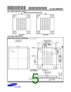
Pin assignment of TBGA A3 ball is changed.
(before) N.C --> (after) Vss
May. 24th 2003
Note : For more detailed features and specifications including FAQ, please refer to Samsung’s Flash web site.
http://www.intl.samsungsemi.com/Memory/Flash/datasheets.html
The attached datasheets are prepared and approved by SAMSUNG Electronics. SAMSUNG Electronics CO., LTD. reserve the right
to change the specifications. SAMSUNG Electronics will evaluate and reply to your requests and questions about device. If you have
any questions, please contact the SAMSUNG branch office near you.
2

 SAMSUNG [ SAMSUNG ]