K9F1208Q0A K9F1216Q0A
K9F1208D0A K9F1216D0A
K9F1208U0A K9F1216U0A
FLASH MEMORY
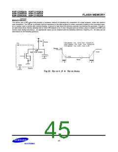
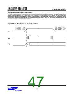
READY/BUSY
The device has a R/B output that provides a hardware method of indicating the completion of a page program, erase and random
read completion. The R/B pin is normally high but transitions to low after program or erase command is written to the command regis-
ter or random read is started after address loading. It returns to high when the internal controller has finished the operation. The pin is
an open-drain driver thereby allowing two or more R/B outputs to be Or-tied. Because pull-up resistor value is related to tr(R/B) and
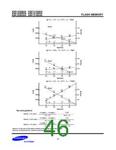
current drain during busy(ibusy) , an appropriate value can be obtained with the following reference chart(Fig 23). Its value can be
determined by the following guidance.
Rp
ibusy
1.8V device - VOL : 0.1V, VOH : VCCq-0.1V
2.65V device - VOL : 0.4V, VOH : Vccq-0.4V
3.3V device - VOL : 0.4V, VOH : 2.4V
VCC
Ready Vcc
R/B
open drain output
VOH
CL
VOL
Busy
tf
tr
GND
Device
Fig 23 Rp vs tr ,tf & Rp vs ibusy
44

 SAMSUNG [ SAMSUNG ]