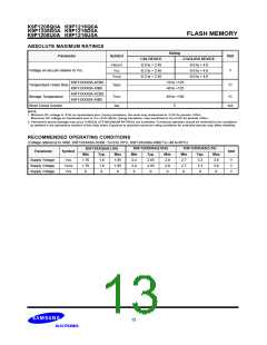
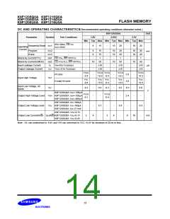
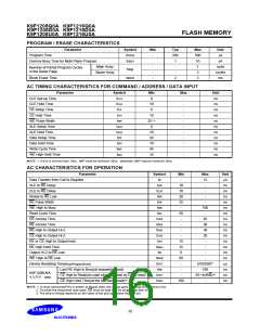
K9F1208Q0A K9F1216Q0A
K9F1208D0A K9F1216D0A
K9F1208U0A K9F1216U0A
FLASH MEMORY
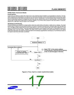
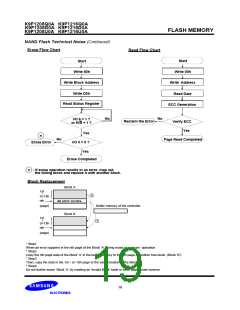
NAND Flash Technical Notes
Invalid Block(s)
Invalid blocks are defined as blocks that contain one or more invalid bits whose reliability is not guaranteed by Samsung. The infor-
mation regarding the invalid block(s) is so called as the invalid block information. Devices with invalid block(s) have the same quality
level as devices with all valid blocks and have the same AC and DC characteristics. An invalid block(s) does not affect the perfor-
mance of valid block(s) because it is isolated from the bit line and the common source line by a select transistor. The system design
must be able to mask out the invalid block(s) via address mapping. The 1st block, which is placed on 00h block address, is fully guar-
anteed to be a valid block, does not require Error Correction.
Identifying Invalid Block(s)
All device locations are erased(FFh) except locations where the invalid block(s) information is written prior to shipping. The invalid
block(s) status is defined by the 6th byte(X8 device) or 1st word(X16 device) in the spare area. Samsung makes sure that either the
1st or 2nd page of every invalid block has non-FFh(X8 device) or non-FFFFh(X16 device) data at the column address of 517(X8
device) or 256 and 261(X16 device). Since the invalid block information is also erasable in most cases, it is impossible to recover the
information once it has been erased. Therefore, the system must be able to recognize the invalid block(s) based on the original
invalid block information and create the invalid block table via the following suggested flow chart(Figure 4). Any intentional erasure of
the original invalid block information is prohibited.
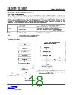
Start
Set Block Address = 0
Increment Block Address
Check "FFh" at the column address
517(X8 device) or 256 and 261(X16 device)
of the 1st and 2nd page in the block
*
No
Create (or update)
Invalid Block(s) Table
Check "FFh" ?
Yes
No
Last Block ?
Yes
End
Figure 4. Flow chart to create invalid block table.
16

 SAMSUNG [ SAMSUNG ]