Preliminary
K5A3x80YT(B)C
MCP MEMORY
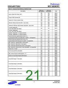
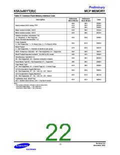
Table 12. Common Flash Memory Interface Code
Addresses
(Word Mode)
Addresses
(Byte Mode)
Description
Data
10H
11H
12H
20H
22H
24H
0051H
0052H
0059H
Query Unique ASCII string "QRY"
13H
14H
26H
28H
0002H
0000H
Primary OEM Command Set
15H
16H
2AH
2CH
0040H
0000H
Address for Primary Extended Table
17H
18H
2EH
30H
0000H
0000H
Alternate OEM Command Set (00h = none exists)
Address for Alternate OEM Extended Table (00h = none exists)
19H
1AH
32H
34H
0000H
0000H
Vcc Min. (write/erase)
D7-D4: volt, D3-D0: 100 millivolt
1BH
1CH
36H
38H
0027H
0036H
Vcc Max. (write/erase)
D7-D4: volt, D3-D0: 100 millivolt
Vpp Min. voltage(00H = no Vpp pin present)
1DH
1EH
1FH
20H
21H
22H
23H
24H
25H
26H
27H
3AH
3CH
3EH
40H
42H
44H
46H
48H
4AH
4CH
4EH
0000H
0000H
0004H
0000H
000AH
0000H
0005H
0000H
0004H
0000H
0016H
Vpp Max. voltage(00H = no Vpp pin present)
Typical timeout per single byte/word write 2N us
Typical timeout for Min. size buffer write 2N us(00H = not supported)
Typical timeout per individual block erase 2N ms
Typical timeout for full chip erase 2N ms(00H = not supported)
Max. timeout for byte/word write 2N times typical
Max. timeout for buffer write 2N times typical
Max. timeout per individual block erase 2N times typical
Max. timeout for full chip erase 2N times typical(00H = not supported)
Device Size = 2N byte
28H
29H
50H
52H
0002H
0000H
Flash Device Interface description
2AH
2BH
54H
56H
0000H
0000H
Max. number of byte in multi-byte write = 2N
Number of Erase Block Regions within device
2CH
58H
0002H
2DH
2EH
2FH
30H
5AH
5CH
5EH
60H
0007H
0000H
0020H
0000H
Erase Block Region 1 Information
Erase Block Region 2 Information
Erase Block Region 3 Information
Erase Block Region 4 Information
31H
32H
33H
34H
62H
64H
66H
68H
003EH
0000H
0000H
0001H
35H
36H
37H
38H
6AH
6CH
6EH
70H
0000H
0000H
0000H
0000H
39H
3AH
3BH
3CH
72H
74H
76H
78H
0000H
0000H
0000H
0000H
Revision 0.0
November 2002
- 21 -

 SAMSUNG [ SAMSUNG ]