Preliminary
K5A3x80YT(B)C
MCP MEMORY
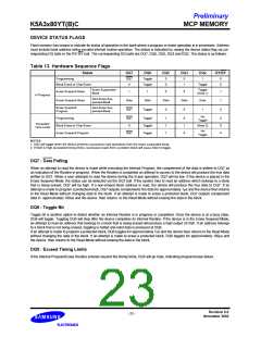
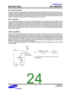
Hardware Reset
Flash memory offers a reset feature by driving the RESET ball to VIL. The RESET ball must be kept low (VIL) for at least 500ns.
When the RESET ball is driven low, any operation in progress will be terminated and the internal state machine will be reset to the
standby mode after 20us. If a hardware reset occurs during a program operation, the data at that particular location will be lost. Once
the RESET ball is taken high, the device requires 200ns of wake-up time until outputs are valid for read access. Also, note that all the
data output balls are tri-stated for the duration of the RESET pulse.
The RESET ball may be tied to the system reset ball. If a system reset occurs during the Internal Program and Erase Routine, the
device will be automatically reset to the read mode ; this will enable the systems microprocessor to read the boot-up firmware from
the Flash memory.
Power-up Protection
To avoid initiation of a write cycle during VccF Power-up, RESET low must be asserted during power-up. After RESET goes high, the
device is reset to the read mode.
Low VccF Write Inhibit
To avoid initiation of a write cycle during VccF power-up and power-down, a write cycle is locked out for VccF less than 1.8V. If VccF
< VLKO (Lock-Out Voltage), the command register and all internal program/erase circuits are disabled. Under this condition the device
will reset itself to the read mode. Subsequent writes will be ignored until the VccF level is greater than VLKO. It is the user¢s responsi-
bility to ensure that the control balls are logically correct to prevent unintentional writes when VccF is above 1.8V.
Write Pulse Glitch Protection
Noise pulses of less than 5ns(typical) on CE , OE, or WE will not initiate a write cycle.
F
Logical Inhibit
Writing is inhibited under any one of the following conditions : OE = VIL, CE = VIH or WE = VIH. To initiate a write, CE and WE must
F
F
be "0", while OE is "1".
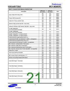
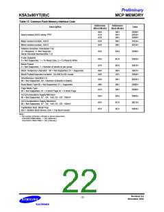
Commom Flash Memory Interface
Common Flash Momory Interface is contrived to increase the compatibility of host system software. It provides the specific informa-
tion of the device, such as memory size, byte/word configuration, and electrical features. Once this information has been obtained,
the system software will know which command sets to use to enable flash writes, block erases, and control the flash component.
When the system writes the CFI command(98H) to address 55H in word mode(or address AAH in byte mode), the device enters the
CFI mode. And then if the system writes the address shown in Table 12, the system can read the CFI data. Query data are always
presented on the lowest-order data outputs(DQ0-7) only. In word(x16) mode, the upper data outputs(DQ8-15) is 00h. To terminate
this operation, the system must write the reset command.
Revision 0.0
November 2002
- 20 -

 SAMSUNG [ SAMSUNG ]