Preliminary
K5A3x80YT(B)C
MCP MEMORY
Multi-Chip Package MEMORY
32M Bit (4Mx8/2Mx16) Dual Bank NOR Flash Memory / 8M(1Mx8/512Kx16) Full CMOS SRAM
FEATURES
GENERAL DESCRIPTION
· Power Supply voltage : 2.7V to 3.3V
· Organization
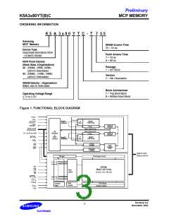
The K5A3x80YT(B)C featuring single 3.0V power supply is a
Multi Chip Package Memory which combines 32Mbit Dual Bank
Flash and 8Mbit fCMOS SRAM.
- Flash : 4,194,304 x 8 / 2,097,152 x 16 bit
- SRAM : 1,048,576 x 8 / 524,288 x 16 bit
· Access Time (@2.7V)
The 32Mbit Flash memory is organized as 4M x8 or 2M x16 bit
and 8Mbit SRAM is organized as 1M x8 or 512K x16 bit. The
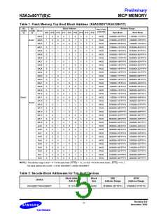
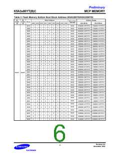
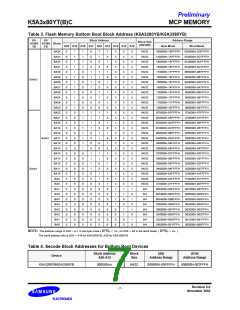
memory architecture of flash memory is designed to divide its
memory arrays into 71 blocks and this provides highly flexible
erase and program capability. This device is capable of reading
data from one bank while programming or erasing in the other
bank with dual bank organization.
- Flash : 70 ns, SRAM : 55 ns
· Power Consumption (typical value)
- Flash Read Current : 14 mA (@5MHz)
Program/Erase Current : 15 mA
Standby mode/Autosleep mode : 5 mA
Read while Program or Read while Erase : 25 mA
- SRAM Operating Current : 22 mA
Standby Current : 0.5 mA
· Secode(Security Code) Block : Extra 64KB Block (Flash)
· Block Group Protection / Unprotection (Flash)
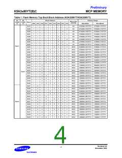
· Flash Bank Size : 8Mb / 24Mb , 16Mb / 16Mb
· Flash Endurance : 100,000 Program/Erase Cycles Minimum
· SRAM Data Retention : 1.5 V (min.)
· Industrial Temperature : -40°C ~ 85°C
· Package : 69-ball TBGA Type - 8 x 11mm, 0.8 mm pitch
1.2mm(max.) Thickness
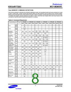
The Flash memory performs a program operation in units of 8 bits
(Byte) or 16 bits (Word) and erases in units of a block. Single or
multiple blocks can be erased. The block erase operation is com-
pleted for typically 0.7sec.
The 8Mbit SRAM supports low data retention voltage for battery
backup operation with low data retention current.
The K5A3x80YT(B)C is suitable for the memory of mobile com-
munication system to reduce mount area. This device is available
in 69-ball TBGA Type package.
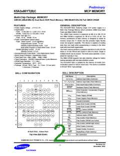
BALL DESCRIPTION
BALL CONFIGURATION
Ball Name
Description
A0 to A18
Address Input Balls (Common)
7
8
9
10
5
6
1
2
3
4
A-1, A19 to A20 Address Input Balls (Flash Memory)
DQ0 to DQ15
RESET
Data Input/Output Balls (Common)
Hardware Reset (Flash Memory)
N.C
N.C
N.C
N.C
N.C
A
B
C
WP/
ACC
LB
A11
A12
A13
A14
A8
A19
A9
A7
Write Protection / Acceleration Program
(Flash Memory)
WE
WP/ACC
CS2
A3
A2
A1
UB
A15
N.C
N.C
A6
A5
A4
RESET
S
Vcc
Vcc
Power Supply (SRAM)
S
Power Supply (Flash Memory)
Ground (Common)
A20
A18 RY/BY
A17
F
D
E
F
Vss
UB
N.C
N.C
A10
N
.C
Upper Byte Enable (SRAM)
Lower Byte Enable (SRAM)
LB
SA
DQ6
A0
DQ1
A16
VSS
OE
N.C
BYTE
BYTE
SA
BYTE Control (SRAM)
S
S
F
DQ15
/A-1
BYTE
DQ13
CE
DQ4
F
DQ9 DQ3
F
G
H
J
BYTE Control (Flash Memory)
F
Address Inputs (SRAM)
Q10 Vcc
Vcc
S
D
Q12
DQ7
CS1
D
Vs
s
DQ0
F
S
CE
Chip Enable (Flash Memory)
Chip Enable (SRAM Low Active)
Chip Enable (SRAM High Active)
Write Enable (Common)
Output Enable (Common)
Ready/Busy (Flash memory)
No Connection
F
E
DQ14
DQ5
DQ11 BYT
DQ8 DQ2
S
CS1
CS2
S
S
N.C
N.C
N.C
N.C
K
WE
OE
69 Ball TBGA , 0.8mm Pitch
Top View (Ball Down)
RY/BY
N.C
SAMSUNG ELECTRONICS CO., LTD. reserves the right to change products and specifications without notice.
Revision 0.0
November 2002
- 2 -

 SAMSUNG [ SAMSUNG ]