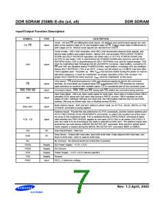
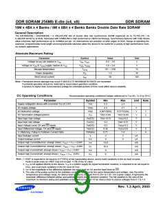
DDR SDRAM 256Mb E-die (x4, x8)
DDR SDRAM
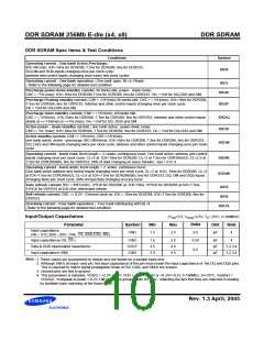
< Detailed test conditions for DDR SDRAM IDD1 & IDD7A >
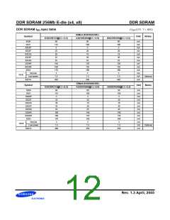
IDD1 : Operating current: One bank operation
1. Only one bank is accessed with tRC(min), Burst Mode, Address and Control inputs on NOP edge are changing once
per clock cycle. lout = 0mA
2. Timing patterns
- B0(133Mhz, CL=2.5) : tCK = 7.5ns, CL=2.5, BL=4, tRCD = 3*tCK, tRC = 9*tCK, tRAS = 6*tCK
Read : A0 N N R0 N N P0 N N A0 N - repeat the same timing with random address changing
*50% of data changing at every burst
- A2 (133Mhz, CL=2) : tCK = 7.5ns, CL=2, BL=4, tRCD = 3*tCK, tRC = 9*tCK, tRAS = 6*tCK
Read : A0 N N R0 N N P0 N N A0 N - repeat the same timing with random address changing
*50% of data changing at every burst
- AA (133Mhz, CL=2) : tCK = 7.5ns, CL=2, BL=4, tRCD = 2*tCK, tRC = 8*tCK, tRAS = 6*tCK
Read : A0 N R0 N N N P0 N A0 N - repeat the same timing with random address changing
*50% of data changing at every burst
- B3(166Mhz, CL=2.5) : tCK=6ns, CL=2.5, BL=4, tRCD=3*tCK, tRC = 10*tCK, tRAS=7*tCK
Read : A0 N N R0 N N P0 N N A0 N - repeat the same timing with random address changing
*50% of data changing at every burst
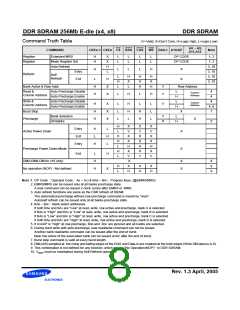
Legend : A=Activate, R=Read, W=Write, P=Precharge, N=NOP
IDD7A : Operating current: Four bank operation
1. Typical Case : Vdd = 2.5V, T=25’ C
2. Worst Case : Vdd = 2.7V, T= 10’ C
3. Four banks are being interleaved with tRC(min), Burst Mode, Address and Control inputs on NOP edge are not
changing. lout = 0mA
4. Timing patterns
- B0(133Mhz, CL=2.5) : tCK = 7.5ns, CL=2.5, BL=4, tRRD = 2*tCK, tRCD = 3*tCK, Read with autoprecharge
Read : A0 N A1 R0 A2 R1 A3 R2 N R3 A0 N A1 R0 - repeat the same timing with random address changing
*50% of data changing at every burst
- AA(133Mhz, CL=2) : tCK = 7.5ns, CL2=2, BL=4, tRRD = 2*tCK, tRCD = 3*tCK, Read with autoprecharge
Read : A0 N A1 R0 A2 R1 A3 R2 A0 R3 A1 R0 - repeat the same timing with random address changing
*50% of data changing at every burst
- A2(133Mhz, CL=2) : tCK = 7.5ns, CL2=2, BL=4, tRRD = 2*tCK, tRCD = 3*tCK, Read with autoprecharge
Read : A0 N A1 R0 A2 R1 A3 R2 N R3 A0 N A1 R0 - repeat the same timing with random address changing
*50% of data changing at every burst
- B3(166Mhz,CL=2.5) : tCK=6ns, CL=2.5, BL=4, tRRD=2*tCK, tRCD=3*tCK, Read with autoprecharge
Read : A0 N A1 R0 A2 R1 A3 R2 N R3 A0 N A1 R0 - repeat the same timing with random address changing
*50% of data changing at every burst
Legend : A=Activate, R=Read, W=Write, P=Precharge, N=NOP
Rev. 1.3 April, 2005

 SAMSUNG [ SAMSUNG ]