DDR SDRAM 256Mb E-die (x4, x8)
DDR SDRAM
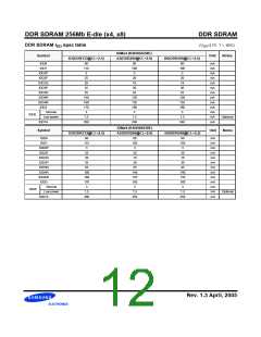
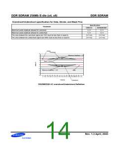
DDR SDRAM Spec Items & Test Conditions
Conditions
Symbol
IDD0
Operating current - One bank Active-Precharge;
tRC=tRCmin; tCK=10ns for DDR200, 7.5ns for DDR266, 6ns for DDR333;
DQ,DM and DQS inputs changing once per clock cycle;
address and control inputs changing once every two clock cycles.
Operating current - One bank operation ; One bank open, BL=4, Reads
- Refer to the following page for detailed test condition
IDD1
Percharge power-down standby current; All banks idle; power - down mode;
CKE = <VIL(max); tCK=10ns for DDR200,7.5ns for DDR266, 6ns for DDR333; Vin = Vref for DQ,DQS and DM.
IDD2P
Precharge Floating standby current; CS# > =VIH(min);All banks idle; CKE > = VIH(min); tCK=10ns for DDR200,
7.5ns for DDR266, 6ns for DDR333; Address and other control inputs changing once per clock cycle;
Vin = Vref for DQ,DQS and DM
IDD2F
Precharge Quiet standby current; CS# > = VIH(min); All banks idle;
CKE > = VIH(min); tCK=10ns for DDR200, 7.5ns for DDR266, 6ns for DDR333; Address and other control inputs
stable at >= VIH(min) or =<VIL(max); Vin = Vref for DQ ,DQS and DM
IDD2Q
IDD3P
Active power - down standby current ; one bank active; power-down mode;
CKE=< VIL (max); tCK=10ns for DDR200, 7.5ns for DDR266, 6ns for DDR333; Vin = Vref for DQ,DQS and DM
Active standby current; CS# >= VIH(min); CKE>=VIH(min);
one bank active; active - precharge; tRC=tRASmax; tCK=10ns for DDR200, 7.5ns for DDR266, 6ns for DDR333;
DQ, DQS and DM inputs changing twice per clock cycle; address and other control inputs changing once per clock
cycle
IDD3N
IDD4R
IDD4W
Operating current - burst read; Burst length = 2; reads; continguous burst; One bank active; address and control
inputs changing once per clock cycle; CL=2 at tCK=10ns for DDR200, CL=2 at 7.5ns for DDR266(A2), CL=2.5 at
7.5ns for DDR266(B0), 6ns for DDR333; 50% of data changing on every transfer; lout = 0 m A
Operating current - burst write; Burst length = 2; writes; continuous burst;
One bank active address and control inputs changing once per clock cycle; CL=2 at tCK= 10ns for DDR200, CL=2
at tCK=7.5ns for DDR266(A2), CL=2.5 at tCK=7.5ns for DDR266(B0), 6ns for DDR333; DQ, DM and DQS inputs
changing twice per clock cycle, 50% of input data changing at every burst
Auto refresh current; tRC = tRFC(min) - 8*tCK for DDR200 at tCK=10ns; 10*tCK for DDR266 at tCK=7.5ns;
12*tCK for DDR333 at tCK=6ns; distributed refresh
IDD5
IDD6
Self refresh current; CKE =< 0.2V; External clock on; tCK = 10ns for DDR200, tCK=7.5ns for DDR266, 6ns for
DDR333.
Orerating current - Four bank operation ; Four bank interleaving with BL=4
-Refer to the following page for detailed test condition
IDD7A
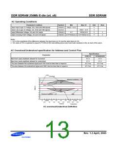
Input/Output Capacitance
(VDD=2.5, VDDQ=2.5V, TA= 25°C, f=100MHz)
Delta
0.5
Parameter
Symbol
Min
Max
Unit
Note
Input capacitance
CIN1
1.5
2.5
pF
4
(A0 ~ A12, BA0 ~ BA1, CKE, CS, RAS,CAS, WE)
Input capacitance( CK, CK )
Data & DQS input/output capacitance
Input capacitance (DM)
CIN2
COUT
CIN3
1.5
3.5
3.5
2.5
4.5
4.5
0.25
pF
pF
pF
4
1,2,3,4
1,2,3,4
0.5
Note :
1.These values are guaranteed by design and are tested on a sample basis only.
2. Although DM is an input -only pin, the input capacitance of this pin must model the input capacitance of the DQ and DQS pins.
This is required to match signal propagation times of DQ, DQS, and DM in the system.
3. Unused pins are tied to ground.
4. This parameteer is sampled. VDDQ = +2.5V +0.2V, VDD = +3.3V +0.3V or +0.25V+0.2V, f=100MHz, tA=25°C, Vout(dc) =
VDDQ/2, Vout(peak to peak) = 0.2V. DM inputs are grouped with I/O pins - reflecting the fact that they are matched in loading
(to facilitate trace matching at the board level).
Rev. 1.3 April, 2005

 SAMSUNG [ SAMSUNG ]