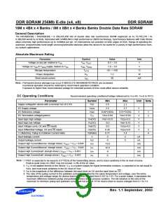
DDR SDRAM 256Mb E-die (x4, x8)
DDR SDRAM
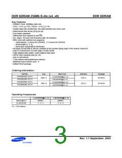
Key Features
• 200MHz Clock, 400Mbps data rate.
• VDD= +2.6V + 0.10V, VDDQ= +2.6V + 0.10V
• Double-data-rate architecture; two data transfers per clock cycle
• Bidirectional data strobe [DQ] (x4,x8)
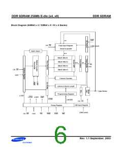
• Four banks operation
• Differential clock inputs(CK and CK)
• DLL aligns DQ and DQS transition with CK transition
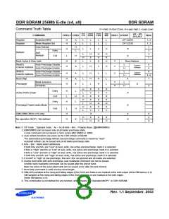
• MRS cycle with address key programs
-. Read latency 3 (clock) for DDR400 , 2.5 (clock) for DDR333
-. Burst length (2, 4, 8)
-. Burst type (sequential & interleave)
• All inputs except data & DM are sampled at the positive going edge of the system clock(CK)
• Data I/O transactions on both edges of data strobe
• Edge aligned data output, center aligned data input
• DM for write masking only (x4, x8)
• Auto & Self refresh
• 7.8us refresh interval(8K/64ms refresh)
• Maximum burst refresh cycle : 8
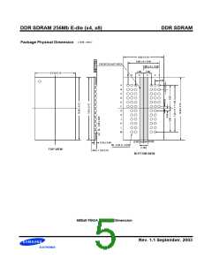
• 60Ball FBGA package
Ordering Information
Part No.
Org.
Max Freq.
CC(DDR400@CL=3)
C4(DDR400@CL=3)
CC(DDR400@CL=3)
C4(DDR400@CL=3)
Interface
Package
K4H560438E-GCCC
K4H560438E-GCC4
K4H560838E-GCCC
K4H560838E-GCC4
64M x 4
SSTL2
60 FBGA
32M x 8
SSTL2
60 FBGA
Operating Frequencies
- CC(DDR400@CL=3)
200MHz
- C4(DDR400@CL=3)
200MHz
Speed @CL3
CL-tRCD-tRP
3 - 3 - 3
3 - 4 - 4
*CL : CAS Latency
Rev. 1.1 September. 2003

 SAMSUNG [ SAMSUNG ]