DDR SDRAM 512Mb C-die (x4, x8, x16)
DDR SDRAM
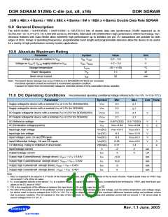
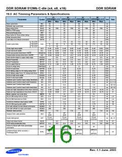
16.0 AC Operating Conditions
Parameter/Condition
Input High (Logic 1) Voltage, DQ, DQS and DM signals
Input Low (Logic 0) Voltage, DQ, DQS and DM signals.
Input Differential Voltage, CK and /CK inputs
Input Crossing Point Voltage, CK and /CK inputs
Note :
Symbol
VIH(AC)
VIL(AC)
VID(AC)
Min
VREF + 0.31
Max
Unit
V
V
V
V
Note
VREF - 0.31
VDDQ+0.6
0.7
1
2
VIX(AC) 0.5*VDDQ-0.2 0.5*VDDQ+0.2
1. VID is the magnitude of the difference between the input level on CK and the input level on /CK.
2. The value of VIX is expected to equal 0.5*VDDQ of the transmitting device and must track variations in the dc level of the same.
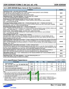
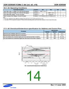
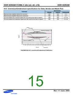
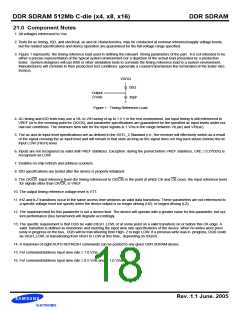
17.0 AC Overshoot/Undershoot specification for Address and Control Pins
Specification
Parameter
DDR400
TBD
DDR333
TBD
DDR200/266
1.5 V
Maximum peak amplitude allowed for overshoot
Maximum peak amplitude allowed for undershoot
TBD
TBD
1.5 V
The area between the overshoot signal and VDD must be less than or equal to
The area between the undershoot signal and GND must be less than or equal to
TBD
TBD
TBD
TBD
4.5 V-ns
4.5 V-ns
VDD
Overshoot
5
4
3
Maximum Amplitude = 1.5V
2
Area = 4.5V-ns
1
0
-1
-2
Maximum Amplitude = 1.5V
GND
-3
-4
-5
0
0.6875
0.5 1.0
1.5
2.5
3.5
4.5
5.5
6.3125
6.0 6.5
undershoot
7.0
2.0
3.0
4.0
5.0
Tims(ns)
AC overshoot/Undershoot Definition
Rev. 1.1 June. 2005

 SAMSUNG [ SAMSUNG ]