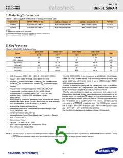
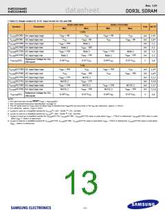
Rev. 1.01
K4B2G0446D
K4B2G0846D
datasheet
DDR3L SDRAM
4. Input/Output Functional Description
[ Table 3 ] Input/Output function description
Symbol
Type
Function
Clock: CK and CK are differential clock inputs. All address and control input signals are sampled on the crossing of
the positive edge of CK and negative edge of CK. Output (read) data is referenced to the crossings of CK and CK
CK, CK
Input
Clock Enable: CKE HIGH activates, and CKE Low deactivates, internal clock signals and device input buffers and
output drivers. Taking CKE Low provides Precharge Power-Down and Self Refresh operation (all banks idle), or
Active Power-Down (Row Active in any bank). CKE is asynchronous for self refresh exit. After VREFCA has become
stable during the power on and initialization sequence, it must be maintained during all operations (including Self-
Refresh). CKE must be maintained high throughout read and write accesses. Input buffers, excluding CK, CK, ODT
and CKE are disabled during power-down. Input buffers, excluding CKE, are disabled during Self -Refresh.
CKE
CS
Input
Chip Select: All commands are masked when CS is registered HIGH. CS provides for external Rank selection on
systems with multiple Ranks. CS is considered part of the command code.
Input
Input
On Die Termination: ODT (registered HIGH) enables termination resistance internal to the DDR3 SDRAM. When
enabled, ODT is only applied to each DQ, DQS, DQS and DM/TDQS, NU/TDQS (When TDQS is enabled via Mode
Register A11=1 in MR1) signal for x8 configurations. The ODT pin will be ignored if the Mode Register (MR1) is pro-
grammed to disable ODT.
ODT
RAS, CAS, WE
Input
Input
Command Inputs: RAS, CAS and WE (along with CS) define the command being entered.
Input Data Mask: DM is an input mask signal for write data. Input data is masked when DM is sampled HIGH coinci-
dent with that input data during a Write access. DM is sampled on both edges of DQS. For x8 device, the function of
DM or TDQS/TDQS is enabled by Mode Register A11 setting in MR1.
DM
(DMU), (DML)
Bank Address Inputs: BA0 - BA2 define to which bank an Active, Read, Write or Precharge command is being
applied. Bank address also determines if the mode register or extended mode register is to be accessed during a
MRS cycle.
BA0 - BA2
A0 - A14
Input
Input
Address Inputs: Provided the row address for Active commands and the column address for Read/Write commands
to select one location out of the memory array in the respective bank. (A10/AP and A12/BC have additional functions,
see below)
The address inputs also provide the op-code during Mode Register Set commands.
Autoprecharge: A10 is sampled during Read/Write commands to determine whether Autoprecharge should be per-
formed to the accessed bank after the Read/Write operation. (HIGH:Autoprecharge; LOW: No Autoprecharge)
A10 is sampled during a Precharge command to determine whether the Precharge applies to one bank (A10 LOW) or
all banks (A10 HIGH). if only one bank is to be precharged, the bank is selected by bank addresses.
A10 / AP
A12 / BC
Input
Burst Chop:A12 is sampled during Read and Write commands to determine if burst chop(on-the-fly) will be per-
formed. (HIGH : no burst chop, LOW : burst chopped). See command truth table for details
Input
Input
Active Low Asynchronous Reset: Reset is active when RESET is LOW, and inactive when RESET is HIGH.
RESET must be HIGH during normal operation. RESET is a CMOS rail to rail signal with DC high and low at 80% and
20% of VDD, i.e.
RESET
DQ
Input/Output Data Input/ Output: Bi-directional data bus.
Data Strobe: Output with read data, input with write data. Edge-aligned with read data, centered in write data. For the
x16, DQSL: corresponds to the data on DQL0-DQL7; DQSU corresponds to the data on DQU0-DQU7. The data
Input/Output strobe DQS, DQSL and DQSU are paired with differential signals DQS, DQSL and DQSU, respectively, to provide dif-
ferential pair signaling to the system during reads and writes. DDR3 SDRAM supports differential data strobe only and
does not support single-ended.
DQS, (DQS)
Termination Data Strobe: TDQS/TDQS is applicable for X8 DRAMs only. When enabled via Mode Register A11=1 in
MR1, DRAM will enable the same termination resistance function on TDQS/TDQS that is applied to DQS/DQS. When
TDQS, (TDQS)
Output
disabled via mode register A11=0 in MR1, DM/TDQS will provide the data mask function and TDQS is not used. x4/
x16 DRAMs must disable the TDQS function via mode register A11=0 in MR1.
NC
No Connect: No internal electrical connection is present.
VDDQ
Supply
Supply
Supply
Supply
Supply
Supply
Supply
DQ Power Supply: 1.35V(1.28V~1.45V) or & 1.5V(1.425V~1.575V)
DQ Ground
VSSQ
VDD
Power Supply: 1.35V(1.28V~1.45V) or & 1.5V(1.425V~1.575V)
Ground
VSS
VREFDQ
VREFCA
ZQ
Reference voltage for DQ
Reference voltage for CA
Reference Pin for ZQ calibration
NOTE : Input only pins (BA0-BA2, A0-A14, RAS, CAS, WE, CS, CKE, ODT and RESET) do not supply termination.
- 9 -

 SAMSUNG [ SAMSUNG ]