Rev. 1.01
K4B2G0446D
K4B2G0846D
datasheet
DDR3L SDRAM
1. Ordering Information
[ Table 1 ] Samsung 2Gb DDR3L D-die ordering information table
DDR3L-1333 (9-9-9)3
K4B2G0446D-HYH9
K4B2G0846D-HYH9
DDR3L-1600 (11-11-11)2
K4B2G0446D-HYK0
K4B2G0846D-HYK0
Organization
512Mx4
DDR3L-1066 (7-7-7)
K4B2G0446D-HYF8
K4B2G0846D-HYF8
Package
78 FBGA
78 FBGA
256Mx8
NOTE :
1. Speed bin is in order of CL-tRCD-tRP.
2. Backward compatible to DDR3L-1333(9-9-9), DDR3L-1066(7-7-7)
3. Backward compatible to DDR3L-1066(7-7-7)
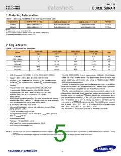
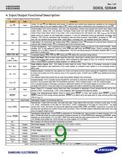
2. Key Features
[ Table 2 ] 2Gb DDR3 D-die Speed bins
DDR3-800
DDR3-1066
7-7-7
DDR3-1333
DDR3-1600
11-11-11
1.25
Speed
6-6-6
Unit
9-9-9
1.5
tCK(min)
CAS Latency
tRCD(min)
tRP(min)
2.5
6
1.875
7
ns
nCK
ns
9
11
15
13.125
13.125
37.5
13.5
13.5
36
13.75
13.75
35
15
ns
tRAS(min)
tRC(min)
37.5
52.5
ns
50.625
49.5
48.75
ns
•
•
JEDEC standard 1.35V(1.28V~1.45V) & 1.5V(1.425V~1.575V)
VDDQ = 1.35V(1.28V~1.45V) & 1.5V(1.425V~1.575V)
The 2Gb DDR3 SDRAM D-die is organized as a 64Mbit x 4 I/Os x 8banks,
32Mbit x 8 I/Os x 8banks device. This synchronous device achieves high
speed double-data-rate transfer rates of up to 1600Mb/sec/pin (DDR3-
1600) for general applications.
The chip is designed to comply with the following key DDR3 SDRAM fea-
tures such as posted CAS, Programmable CWL, Internal (Self) Calibration,
On Die Termination using ODT pin and Asynchronous Reset .
All of the control and address inputs are synchronized with a pair of exter-
nally supplied differential clocks. Inputs are latched at the crosspoint of dif-
ferential clocks (CK rising and CK falling). All I/Os are synchronized with a
pair of bidirectional strobes (DQS and DQS) in a source synchronous fash-
ion. The address bus is used to convey row, column, and bank address
information in a RAS/CAS multiplexing style. The DDR3 device operates
with a single 1.35V(1.28V~1.45V) or 1.5V(1.425V~1.575V) power supply
and 1.35V(1.28V~1.45V) or 1.5V(1.425V~1.575V).
•
400 MHz fCK for 800Mb/sec/pin, 533MHz fCK for 1066Mb/sec/pin,
667MHz fCK for 1333Mb/sec/pin, 800MHz fCK for 1600Mb/sec/pin
•
•
•
•
8 Banks
Programmable CAS Latency(posted CAS): 5,6,7,8,9,10,11
Programmable Additive Latency: 0, CL-2 or CL-1 clock
Programmable CAS Write Latency (CWL) = 5(DDR3-800),
6(DDR3-1066), 7(DDR3-1333) and 8(DDR3-1600)
•
•
8-bit pre-fetch
Burst Length: 8 (Interleave without any limit, sequential with starting
address “000” only), 4 with tCCD = 4 which does not allow seamless
read or write [either On the fly using A12 or MRS]
•
•
Bi-directional Differential Data-Strobe
Internal(self) calibration : Internal self calibration through ZQ pin
(RZQ : 240 ohm ± 1%)
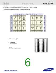
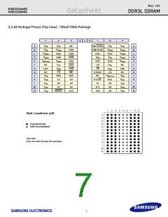
The 2Gb DDR3 D-die device is available in 78ball FBGAs(x4/x8)
•
•
On Die Termination using ODT pin
Average Refresh Period 7.8us at lower than TCASE 85°C, 3.9us at
85°C < TCASE < 95 °C
•
•
•
•
Asynchronous Reset
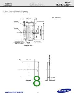
Package : 78 balls FBGA - x4/x8
All of Lead-Free products are compliant for RoHS
All of products are Halogen-free
NOTE : 1. This data sheet is an abstract of full DDR3 specification and does not cover the common features which are described in “DDR3 SDRAM Device Operation & Timing
Diagram”.
2. The functionality described and the timing specifications included in this data sheet are for the DLL Enabled mode of operation.
- 5 -

 SAMSUNG [ SAMSUNG ]