Rev. 1.01
K4B2G0446D
K4B2G0846D
datasheet
DDR3L SDRAM
Table Of Contents
2Gb D-die DDR3L SDRAM
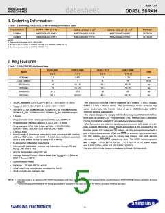
1. Ordering Information.....................................................................................................................................................5
2. Key Features.................................................................................................................................................................5
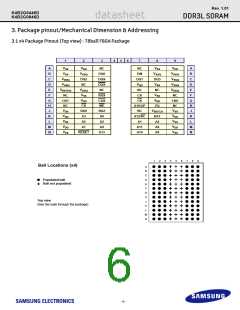
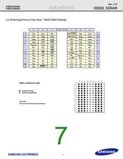
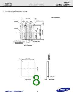
3. Package pinout/Mechanical Dimension & Addressing..................................................................................................6
3.1 x4 Package Pinout (Top view) : 78ball FBGA Package .......................................................................................... 6
3.2 x8 Package Pinout (Top view) : 78ball FBGA Package .......................................................................................... 7
3.3 FBGA Package Dimension (x4/x8).......................................................................................................................... 8
4. Input/Output Functional Description..............................................................................................................................9
5. DDR3 SDRAM Addressing ...........................................................................................................................................10
6. Absolute Maximum Ratings ..........................................................................................................................................11
6.1 Absolute Maximum DC Ratings............................................................................................................................... 11
6.2 DRAM Component Operating Temperature Range ................................................................................................ 11
7. AC & DC Operating Conditions.....................................................................................................................................11
7.1 Recommended DC operating Conditions (SSTL_1.5)............................................................................................. 11
8. AC & DC Input Measurement Levels............................................................................................................................12
8.1 AC & DC Logic input levels for single-ended signals .............................................................................................. 12
8.2 VREF Tolerances...................................................................................................................................................... 14
8.3 AC & DC Logic Input Levels for Differential Signals................................................................................................ 15
8.3.1. Differential signals definition ............................................................................................................................ 15
8.3.2. Differential swing requirement for clock (CK - CK) and strobe (DQS - DQS) .................................................. 15
8.3.3. Single-ended requirements for differential signals........................................................................................... 17
8.4 Differential Input Cross Point Voltage...................................................................................................................... 18
8.5 Slew rate definition for Differential Input Signals..................................................................................................... 19
8.6 Slew rate definitions for Differential Input Signals ................................................................................................... 19
9. AC & DC Output Measurement Levels .........................................................................................................................19
9.1 Single-ended AC & DC Output Levels..................................................................................................................... 19
9.2 Differential AC & DC Output Levels......................................................................................................................... 19
9.3 Single-ended Output Slew Rate .............................................................................................................................. 20
9.4 Differential Output Slew Rate .................................................................................................................................. 21
9.5 Reference Load for AC Timing and Output Slew Rate............................................................................................ 21
9.6 Overshoot/Undershoot Specification....................................................................................................................... 22
9.6.1. Address and Control Overshoot and Undershoot specifications...................................................................... 22
9.6.2. Clock, Data, Strobe and Mask Overshoot and Undershoot Specifications...................................................... 23
9.7 34ohm Output Driver DC Electrical Characteristics................................................................................................. 23
9.7.1. Output Drive Temperature and Voltage Sensitivity.......................................................................................... 25
9.8 On-Die Termination (ODT) Levels and I-V Characteristics ..................................................................................... 25
9.8.1. ODT DC Electrical Characteristics................................................................................................................... 26
9.8.2. ODT Temperature and Voltage sensitivity ...................................................................................................... 28
9.9 ODT Timing Definitions ........................................................................................................................................... 29
9.9.1. Test Load for ODT Timings.............................................................................................................................. 29
9.9.2. ODT Timing Definitions.................................................................................................................................... 29
10. IDD Current Measure Method.....................................................................................................................................32
10.1 IDD Measurement Conditions ............................................................................................................................... 32
11. 2Gb DDR3 SDRAM D-die IDD Specification Table ....................................................................................................41
12. Input/Output Capacitance ...........................................................................................................................................42
13. Electrical Characteristics and AC timing for DDR3-800 to DDR3-1600......................................................................43
13.1 Clock Specification ................................................................................................................................................ 43
13.1.1. Definition for tCK(avg).................................................................................................................................... 43
13.1.2. Definition for tCK(abs).................................................................................................................................... 43
13.1.3. Definition for tCH(avg) and tCL(avg).............................................................................................................. 43
13.1.4. Definition for note for tJIT(per), tJIT(per, Ick)................................................................................................. 43
13.1.5. Definition for tJIT(cc), tJIT(cc, Ick) ................................................................................................................. 43
13.1.6. Definition for tERR(nper)................................................................................................................................ 43
13.2 Refresh Parameters by Device Density................................................................................................................. 44
13.3 Speed Bins and CL, tRCD, tRP, tRC and tRAS for corresponding Bin................................................................. 44
13.3.1. Speed Bin Table Notes .................................................................................................................................. 47
- 3 -

 SAMSUNG [ SAMSUNG ]