Rev. 1.01
K4B2G0446D
K4B2G0846D
datasheet
DDR3L SDRAM
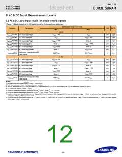
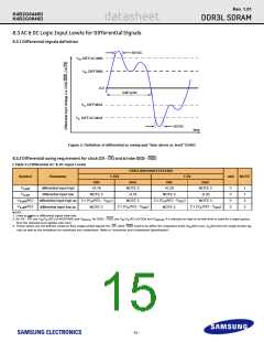
8.3 AC & DC Logic Input Levels for Differential Signals
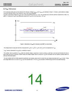
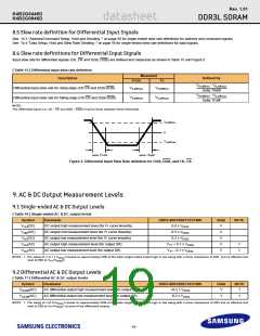
8.3.1 Differential signals definition
tDVAC
VIH.DIFF.AC.MIN
VIH.DIFF.MIN
0.0
half cycle
VIL.DIFF.MAX
VIL.DIFF.AC.MAX
tDVAC
time
Figure 2. Definition of differential ac-swing and "time above ac level" tDVAC
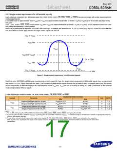
8.3.2 Differential swing requirement for clock (CK - CK) and strobe (DQS - DQS)
[ Table 9 ] Differential AC & DC Input Levels
DDR3-800/1066/1333/1600
Symbol
Parameter
1.35V
1.5V
unit
NOTE
min
+0.18
max
NOTE 3
min
+0.20
max
NOTE 3
VIHdiff
VILdiff
differential input high
differential input low
V
V
V
V
1
1
2
2
NOTE 3
-0.18
NOTE 3
-0.20
V
IHdiff(AC)
ILdiff(AC)
2 x (VIH(AC) - VREF
NOTE 3
)
2 x (VIH(AC) - VREF
NOTE 3
)
differential input high ac
differential input low ac
NOTE 3
NOTE 3
V
2 x (VIL(AC) - VREF
)
2 x (VIL(AC) - VREF)
NOTE :
1. Used to define a differential signal slew-rate.
2. for CK - CK use V /V (AC) of ADD/CMD and V
IH IL
; for DQS - DQS use V /V (AC) of DQs and V
; if a reduced ac-high or ac-low level is used for a signal group,
REFCA
IH IL
REFDQ
then the reduced level applies also here.
3. These values are not defined, however they single-ended signals CK, CK, DQS, DQS need to be within the respective limits (V (DC) max, V (DC)min) for single-ended sig-
IH
IL
nals as well as the limitations for overshoot and undershoot. Refer to "overshoot and Undersheet Specification"
- 15 -

 SAMSUNG [ SAMSUNG ]