Technical Note
BU2098F, BU2090F, BU2090FS
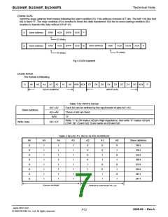
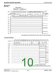
○Write DATA
Send the stave address from master following the start condition (S). This address consists of 7 bits. The left 1 bit (the foot
bit) is fixed “0”. The stop condition (P) is needed to finish the data transferred. But the re-send starting condition (Sr)
enables to transfer the data without STOP (P).
slave address
R/W
ACK
ACK
DATA
S
P
“0” (Write)
ACK
DATA
slave address
DATA
slave address
R/W
ACK Sr
R/W
ACK
ACK
P
S
“0” (Write)
“0” (Write)
Fig.4 DATA transmit
○Data format
The format is following.
S
A6
A5
A4
A3
A2
A1
A0 R/W ACK D7
D6
D5
D4
D3 D2
D1
D0 ACK
P
SLAVE ADDRESS
WRITE DATA
Table 1 for WRITE format
A0~A2
A3~A6
R/W
Each bit can be defined by the input levels of pins A0~A3.
Slave address
These 4 bits are fixed.
“0”
Write “1” to D0 makes Q0 pin High-impedance. And write “0” makes Q0 pin
LOW. D[1:7] and Q[1:7] are same as D0 and Q0.
Write Data
D0~D7
Table 2 for (A2, A1, A0) to SLAVE ADDRESS
A6
0
A5
1
A4
A3
1
A2
0
A1
0
A0
0
Slave address
38H
1
1
1
1
1
1
1
1
0
1
1
0
0
1
39H
0
1
1
0
1
0
3AH
0
1
1
0
1
1
3BH
0
1
1
1
0
0
3CH
0
1
1
1
0
1
3DH
0
1
1
1
1
0
3EH
0
1
1
1
1
1
3FH
Fixed for BU2098F
Defined by external pin A0~A2
www.rohm.com
© 2009 ROHM Co., Ltd. All rights reserved.
2009.06 - Rev.A
7/12

 ROHM [ ROHM ]