Technical Note
BU2098F, BU2090F, BU2090FS
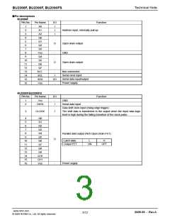
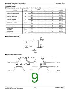
●Pin descriptions
BU2098F
PIN No.
Pin Name
A0
I/O
Function
1
2
I
I
I
A1
Address input, internally pull-up
3
A2
4
Q0
5
Q1
O
-
Open drain output
GND
6
Q2
7
Q3
8
VSS
Q4
9
10
11
12
13
14
15
16
Q5
O
Open drain output
Q6
Q7
N.C.
SCL
SDA
VDD
-
I
Non connected
Serial clock input
Serial data input/output
Power supply
I/O
-
BU2090F/BU2090FS
PIN No.
Pin Name
I/O
Function
1
2
VSS
-
I
GND
DATA
Serial data input
Data shift clock input (rising edge trigger)
3
CLOCK
I
The shift data is transferred to the output when the input data logic
level is high during the falling transition of the clock pulse.
4
5
Q0
Q1
6
Q2
7
Q3
8
Q4
Parallel data output (Nch Open Drain FET)
9
Q5
O
Latch data
L
H
10
11
12
13
14
15
16
Q6
Output FET
ON
OFF
Q7
Q8
Q9
Q10
Q11
VDD
Power supply
-
www.rohm.com
2009.06 - Rev.A
3/12
© 2009 ROHM Co., Ltd. All rights reserved.

 ROHM [ ROHM ]