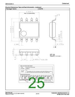
Datasheet
BR24G08-3
Power Up/Down Conditions
At power on, the IC’s internal circuits may go through unstable low voltage area as the VCC rises, making the IC’s internal
logic circuit not completely reset, hence, malfunction may occur. To prevent this, the IC is equipped with POR circuit and
LVCC circuit. To assure the operation, observe the following conditions at power on.
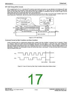
1. Set SDA = 'H' and SCL ='L' or 'H’
2. Start power source so as to satisfy the recommended conditions of tR, tOFF, and Vbot for operating POR circuit.
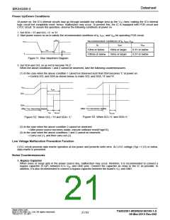
tR
Recommended conditions of tR, tOFF,Vbot
VCC
tR
tOFF
Vbot
10ms or below
100ms or below
10ms or larger
10ms or larger
0.3V or below
0.2V or below
tOFF
Vbot
0
Figure 51. Rise Waveform Diagram
3. Set SDA and SCL so as not to become 'Hi-Z'.
When the above conditions 1 and 2 cannot be observed, take the following countermeasures.
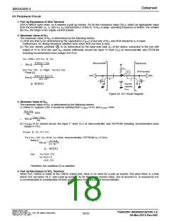
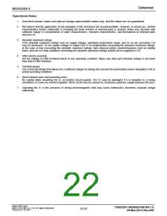
(1) In the case when the above condition 1 cannot be observed such that SDA becomes 'L' at power on .
→Control SCL and SDA as shown below, to make SCL and SDA, 'H' and 'H'.
VCC
tLOW
SCL
SDA
After Vcc becomes stable
After Vcc becomes stable
tDH
tSU:DAT
tSU:DAT
Figure 53. When SCL='L' and SDA='L'
Figure 52. When SCL= 'H' and SDA= 'L'
(2) In the case when the above condition 2 cannot be observed.
→After power source becomes stable, execute software reset(Page16).
(3) In the case when the above conditions 1 and 2 cannot be observed.
→Carry out (1), and then carry out (2).
Low Voltage Malfunction Prevention Function
LVCC circuit prevents data rewrite operation at low power and prevents write error. At LVCC voltage (Typ =1.2V) or below,
data rewrite is prevented.
Noise Countermeasures
1. Bypass Capacitor
When noise or surge gets in the power source line, malfunction may occur, therefore, it is recommended to connect a
bypass capacitor (0.1µF) between IC’s VCC and GND pins. Connect the capacitor as close to the IC as possible. In
addition, it is also recommended to connect a bypass capacitor between the board’s VCC and GND.
www.rohm.com
TSZ02201-0R2R0G100190-1-2
09.Mar.2013 Rev.002
©2013 ROHM Co., Ltd. All rights reserved.
21/33
TSZ22111・15・001

 ROHM [ ROHM ]