Datasheet
BR24G08-3
Cautions on Microcontroller Connection
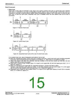
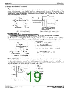
1. RS
In I2C BUS, it is recommended that SDA port is of open drain input/output. However, when using CMOS input / output of
tri state to SDA port, insert a series resistance RS between the pull up resistance RPU and the SDA terminal of EEPROM.
This is to control over current that may occur when PMOS of the microcontroller and NMOS of EEPROM are turned ON
simultaneously. RS also plays the role of protecting the SDA terminal against surge. Therefore, even when SDA port is
open drain input/output, RS can be used.
ACK
SCL
RPU
RS
SDA
'H' output of microcontroller
'L' output of EEPROM
EEPROM
Microcontroller
Over current flows to SDA line by 'H'
output of microcontroller and 'L'
output of EEPROM.
Figure 45. I/O circuit diagram
Figure 46. Input / output collision timing
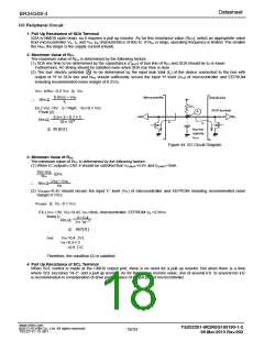
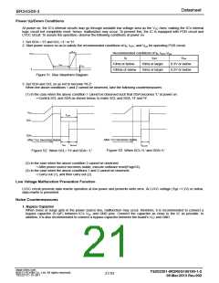
2. Maximum Value of Rs
The maximum value of Rs is determined by the following relations.
(1) SDA rise time to be determined by the capacitance (CBUS) of bus line of RPU and SDA should be tR or lower.
Furthermore, AC timing should be satisfied even when SDA rise time is low.
(2) The bus electric potential
should sufficiently secure the input 'L' level (VIL) of microcontroller including recommended noise margin 0.1Vcc.
A to be determined by RPU and RS the moment when EEPROM outputs 'L' to SDA bus
○
(Vcc-VOL)×RS +VOL+0.1Vcc≦VIL
VCC
RPU+RS
A
RPU
VIL-VOL-0.1Vcc
×RPU
∴
RS≦
RS
1.1Vcc-VIL
VOL
IOL
Ex)VCC=3V VIL=0.3VCC VOL=0.4V RPU=20kΩ
Bus line
capacity
CBUS
0.3×3-0.4-0.1×3
×20×103
RS≦
1.1×3-0.3×3
VIL
EEPROM
Micro controller
≦1.67[kΩ]
Figure 47. I/O Circuit Diagram
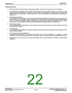
3. Minimum Value of Rs
The minimum value of RS is determined by over current at bus collision. When over current flows, noises in power source
line and instantaneous power failure of power source may occur. When allowable over current is defined as I, the
following relation must be satisfied. Determine the allowable current in consideration of the impedance of power source
line in set and so forth. Set the over current to EEPROM at 10mA or lower.
Vcc
RS
≦I
RPU
RS
Vcc
I
∴
RS≧
'L'output
EX) VCC=3V I=10mA
3
Over current I
RS≧
3
10×10-
'H' output
≧300[Ω]
EEPROM
Microcontroller
Figure 48. I/O Circuit Diagram
www.rohm.com
TSZ02201-0R2R0G100190-1-2
09.Mar.2013 Rev.002
©2013 ROHM Co., Ltd. All rights reserved.
19/33
TSZ22111・15・001

 ROHM [ ROHM ]