Technical Note
BA2904YF-C,BA2904YFVM-C,BA2902YF-C,BA2902YFV-C
●Notes for use
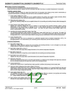
1) Unused circuits
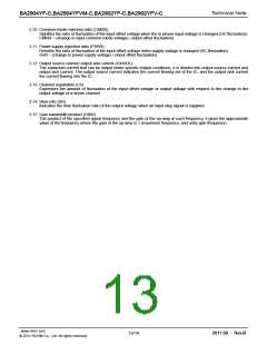
VCC
When there are unused circuits, it is recommended that they be connected
as in Fig.56, setting the non-inverting input terminal to a potential within the
in-phase input voltage range (Vicm).
Please keep this
同相入力電圧
potencial in Vicm
範囲内の電位
2) Input voltage
Applying VEE+36[V] to the input terminal is possible without causing
deterioration of the electrical characteristics or destruction, irrespective of
the supply voltage. However, this does not ensure normal circuit operation.
Please note that the circuit operates normally only when the input voltage
is within the common mode input voltage range of the electric
characteristics.
VEE
Fig. 56 Example of processing unused circuit
3) Power supply (single / dual)
The op-amp operates when the voltage supplied is between VCC and VEE Therefore, the single supply op-mp can be
used as a dual supply op-amp as well.
4) Power dissipation (Pd)
Using the unit in excess of the rated power dissipation may cause deterioration in electrical characteristics due to the rise
in chip temperature, including reduced current capability. Therefore, please take into consideration the power dissipation
(Pd) under actual operating conditions and apply a sufficient margin in thermal design. Refer to the thermal derating
curves for more information.
5) Short-circuit between pins and erroneous mounting
Incorrect mounting may damage the IC. In addition, the presence of foreign substances between the outputs, the output
and the power supply, or the output and GND may result in IC destruction.
6) Operation in a strong electromagnetic field
Operation in a strong electromagnetic field may cause malfunctions.
7) Radiation
This IC is not designed to withstand radiation.
8) IC handing
Applying mechanical stress to the IC by deflecting or bending the board may cause fluctuation of the electrical
characteristics due to piezoelectric (piezo) effects.
9) IC operation
The output stage of the IC is configured using Class C push-pull circuits. Therefore, when the load resistor is connected to
the middle potential of VCC and VEE, crossover distortion occurs at the changeover between discharging and charging of
the output current. Connecting a resistor between the output terminal and GND, and increasing the bias current for Class
A operation will suppress crossover distortion.
10) Board inspection
Connecting a capacitor to a pin with low impedance may stress the IC. Therefore, discharging the capacitor after every
process is recommended. In addition, when attaching and detaching the jig during the inspection phase, ensure that the
power is turned OFF before inspection and removal. Furthermore, please take measures against ESD in the assembly
process as well as during transportation and storage.
11) Output capacitor
Discharge of the external output capacitor to VCC is possible via internal parasitic elements when VCC is shorted to VEE,
causing damage to the internal circuitry due to thermal stress. Therefore, when using this IC in circuits where oscillation
due to output capacitive load does not occur, such as in voltage comparators, use an output capacitor with a capacitance
less than 0.1μF.
12) Oscillation by output capacitor
Please pay attention to oscillation by output capacitor, designing application of negative feed back loop circuit with these
ICs.
www.rohm.com
2011.08 - Rev.B
14/16
© 2011 ROHM Co., Ltd. All rights reserved.

 ROHM [ ROHM ]