Technical Note
BA2904YF-C,BA2904YFVM-C,BA2902YF-C,BA2902YFV-C
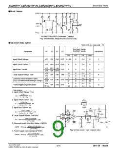
●Circuit Diagram
VCC
IN
IN
-
+
VOUT
VEE
BA2904Y / BA2902Y Schematic Diagram
Fig. 49 Schematic Diagram (one channel only)
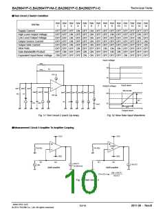
●Test circuit1 NULL method
VCC,VEE,EK,Vicm Unit:[V]
BA2904Y family
BA2902Y family
VF
S1
S2
S3
calculation
Parameter
Vcc
ON OFF 5~30
VEE
0
EK
Vicm
0
Input Offset Voltage
Input Offset Current
Input Bias Current
VF1 ON
-1.4
1
2
3
4
5
6
VF2 OFF OFF OFF
5
5
0
0
-1.4
-1.4
0
0
VF3 OFF ON
OFF
VF4 ON OFF
VF5
15
15
5
0
0
0
0
0
0
-1.4
-11.4
-1.4
-1.4
-1.4
-1.4
0
0
Large Signal Voltage Gain
ON
ON
ON
ON
ON
VF6
VF7
VF8
VF9
VF10
0
Common-mode Rejection Ratio
(Input common-mode Voltage Range)
ON OFF
ON OFF
5
3.5
0
5
Power Supply Rejection Ratio
30
0
- Calculation -
1. Input Offset Voltage (Vio)
| VF1 |
[V]
Vio =
1 + Rf / Rs
C2
0.1[μF]
2. Input Offset Current (Iio)
| VF2 VF1 |
-
[A]
Iio =
Ri ×(1 + Rf / Rs)
Rf
50[kΩ]
3. Input Bias Current (Ib)
C1
RK
S1
Ri
VCC
| VF4 VF3 |
-
500[kΩ]
0.1[μF]
+15[V]
EK
[A]
Ib =
2×Ri× (1 + Rf / Rs)
Rs
4. Large Signal Voltage Gain (Av)
RK 500[kΩ]
50[Ω] 10[kΩ]
DUT
VEE
10[kΩ]
50[Ω]
NULL
EK×(1+Rf /Rs)
Δ
S3
RL
Av = 20×Log
Ri
Rs
[dB]
C3
1000[pF]
|VF5-VF6|
VF
V
S2
-15[V]
Vicm
5. Common-mode Rejection Ration (CMRR)
Vicm×(1+Rf/Rs)
|VF8-VF7|
Δ
CMRR = 20×Log
[dB]
Fig. 50 Test circuit1 (one channel only)
6. Power supply rejection ratio (PSRR)
Vcc×(1+Rf /Rs)
|VF10-VF9|
Δ
PSRR = 20×Log
[dB]
www.rohm.com
© 2011 ROHM Co., Ltd. All rights reserved.
2011.08 - Rev.B
9/16

 ROHM [ ROHM ]