Technical Note
BA2904YF-C,BA2904YFVM-C,BA2902YF-C,BA2902YFV-C
●Description of Electrical Characteristics
Described below are descriptions of the relevant electrical terms
Please note that item names, symbols and their meanings may differ from those on another manufacturer’s documents.
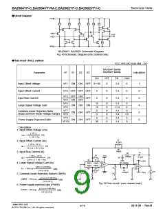
1.Absolute maximum ratings
The absolute maximum ratings are values that should never be exceeded, since doing so may result in deterioration of
electrical characteristics or damage to the part itself as well as peripheral components.
1.1 Power supply voltage (VCC-VEE)
Expresses the maximum voltage that can be supplied between the positive and negative supply terminals without
causing deterioration of the electrical characteristics or destruction of the internal circuitry.
1.2 Differential input voltage (Vid)
Indicates the maximum voltage that can be supplied between the non-inverting and inverting terminals without damaging the
IC.
1.3 Input common-mode voltage range (Vicm)
Signifies the maximum voltage that can be supplied to non-inverting and inverting terminals without causing
deterioration of the characteristics or damage to the IC itself. Normal operation is not guaranteed within the
common-mode voltage range of the maximum ratings – use within the input common-mode voltage range of the
electric characteristics instead.
1.4 Operating and storage temperature ranges (Topr,Tstg)
The operating temperature range indicates the temperature range within which the IC can operate. The higher the
ambient temperature, the lower the power consumption of the IC. The storage temperature range denotes the range
of temperatures the IC can be stored under without causing excessive deterioration of the electrical characteristics.
1.5 Power dissipation (Pd)
Indicates the power that can be consumed by a particular mounted board at ambient temperature (25℃). For
packaged products, Pd is determined by the maximum junction temperature and the thermal resistance.
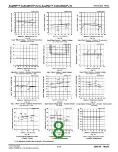
2.Electrical characteristics
2.1 Input offset voltage (Vio)
Signifies the voltage difference between the non-inverting and inverting terminals. It can be thought of as the input
voltage difference required for setting the output voltage to 0 V.
2.2 Input offset voltage drift (△Vio/△T)
Denotes the ratio of the input offset voltage fluctuation to the ambient temperature fluctuation.
2.3 Input offset current (Iio)
Indicates the difference of input bias current between the non-inverting and inverting terminals.
2.4 Input offset current drift (△Iio/△T)
Signifies the ratio of the input offset current fluctuation to the ambient temperature fluctuation.
2.5 Input bias current (Ib)
Denotes the current that flows into or out of the input terminal, it is defined by the average of the input bias current at
the non-inverting terminal and the input bias current at the inverting terminal.
2.6 Circuit current (ICC)
Indicates the current of the IC itself that flows under specified conditions and during no-load steady state.
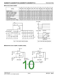
2.7 High level output voltage/low level output voltage (VOH/VOL)
Signifying the voltage range that can be output under specified load conditions, it is in general divided into high level
output voltage and low level output voltage. High level output voltage indicates the upper limit of the output voltage,
while low level output voltage the lower limit.
2.8 Large signal voltage gain (AV)
The amplifying rate (gain) of the output voltage against the voltage difference between non-inverting and inverting
terminals, it is (normally) the amplifying rate (gain) with respect to DC voltage.
AV = (output voltage fluctuation) / (input offset fluctuation)
2.9 Input common-mode voltage range (Vicm)
Indicates the input voltage range under which the IC operates normally.
www.rohm.com
© 2011 ROHM Co., Ltd. All rights reserved.
2011.08 - Rev.B
12/16

 ROHM [ ROHM ]