AD8510/AD8512/AD8513
PRECISION RECTIFIERS
Rectifying circuits are used in a multitude of applications. One
of the most popular uses is in the design of regulated power
supplies, where a rectifier circuit is used to convert an input
sinusoid to a unipolar output voltage.
However, there are some potential problems with amplifiers
used in this manner. When the input voltage (VIN) is negative,
the output is zero, and the magnitude of VIN is doubled at the
inputs of the op amp. If this voltage exceeds the power supply
voltage, it may permanently damage some amplifiers. In addition,
the op amp must come out of saturation when VIN is negative.
This delays the output signal because the amplifier requires
time to enter its linear region.
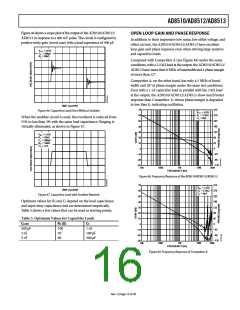
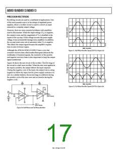
TIME (1ms/DIV)
Although the AD8510/AD8512/AD8513 have a very fast
overdrive recovery time, which makes them great choices for the
rectification of transient signals, the symmetry of the positive
and negative recovery times is also important to keep the output
signal undistorted.
Figure 51. Half-Wave Rectifier Signal (OUT A in Figure 50)
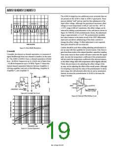
Figure 50 shows the test circuit of the rectifier. The first stage of
the circuit is a half-wave rectifier. When the sine wave applied at
the input is positive, the output follows the input response.
During the negative cycle of the input, the output tries to swing
negative to follow the input, but the power supply restrains it to
zero. In a similar fashion, the second stage is a follower during
the positive cycle of the sine wave and an inverter during the
negative cycle.
R2
R3
10kΩ
10kΩ
TIME (1ms/DIV)
Figure 52. Full-Wave Rectifier Signal (OUT B in Figure 50)
10V
V
IN
3V p-p
6
5
4
2/2
7
3
2
AD8512
8
1/2
OUT B
(FULL WAVE)
R1
1kΩ
8
1
AD8512
4
10V
OUT A
(HALF WAVE)
Figure 50. Half-Wave and Full-Wave Rectifiers
Rev. I | Page 16 of 20

 ROCHESTER [ Rochester Electronics ]