AD8510/AD8512/AD8513
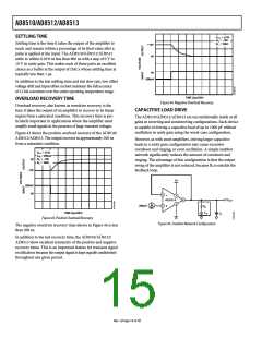
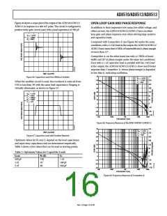
Figure 46 shows a scope plot of the output of the AD8510/AD8512/
AD8513 in response to a 400 mV pulse. The circuit is configured in
positive unity gain (worst case) with a load experience of 500 pF.
OPEN-LOOP GAIN AND PHASE RESPONSE
In addition to their impressive low noise, low offset voltage, and
offset current, the AD8510/AD8512/AD8513 have excellent
loop gain and phase response even when driving large resistive
and capacitive loads.
V
= ±15V
= 500pF
=10kΩ
SY
C
L
R
L
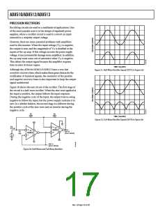
Compared with Competitor A (see Figure 49) under the same
conditions, with a 2.5 kΩ load at the output, the AD8510/AD8512/
AD8513 have more than 8 MHz of bandwidth and a phase margin
of more than 52°.
Competitor A, on the other hand, has only 4.5 MHz of band-
width and 28° of phase margin under the same test conditions.
Even with a 1 nF capacitive load in parallel with the 2 kΩ load
at the output, the AD8510/AD8512/AD8513 show much better
response than Competitor A, whose phase margin is degraded
to less than 0, indicating oscillation.
TIME (1µs/DIV)
70
315
270
225
180
Figure 46. Capacitive Load Drive Without Snubber
V
R
C
= ±15V
= 2.5kΩ
= 0pF
SY
60
L
L
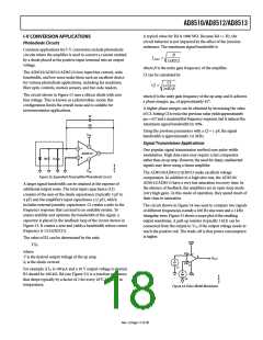
When the snubber circuit is used, the overshoot is reduced from
55% to less than 3% with the same load capacitance. Ringing is
virtually eliminated, as shown in Figure 47.
50
40
30
20
10
135
90
V
= ±15V
= 10kΩ
= 500pF
= 100Ω
= 1nF
SY
R
C
R
C
L
L
S
S
45
0
0
–10
–20
–30
–45
–90
–135
50M
10k
100k
1M
10M
FREQUENCY (Hz)
Figure 48. Frequency Response of the AD8510/AD8512/AD8513
70
315
270
225
180
V
R
C
= ±15V
= 2.5kΩ
= 0pF
SY
TIME (1µs/DIV)
60
L
L
Figure 47. Capacitive Load with Snubber Network
50
40
30
20
10
Optimum values for RS and CS depend on the load capacitance
and input stray capacitance and are determined empirically.
Table 5 shows a few values that can be used as starting points.
135
90
Table 5. Optimum Values for Capacitive Loads
45
CLOAD
500 pF
2 nF
RS (Ω)
100
70
CS
0
0
–10
–20
–30
1 nF
100 pF
300 pF
–45
–90
5 nF
60
–135
50M
10k
100k
1M
10M
FREQUENCY (Hz)
Figure 49. Frequency Response of Competitor A
Rev. I | Page 15 of 20

 ROCHESTER [ Rochester Electronics ]