AD8510/AD8512/AD8513
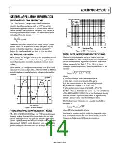
SETTLING TIME
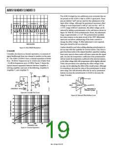
V
A
R
= ±15V
= –100
= 10kΩ
SY
V
L
Settling time is the time it takes the output of the amplifier to
reach and remain within a percentage of its final value after a
pulse is applied at the input. The AD8510/AD8512/AD8513
settle to within 0.01% in less than 900 ns with a step of 0 V to
10 V in unity gain. This makes each of these parts an excellent
choice as a buffer at the output of DACs whose settling time is
typically less than 1 μs.
+15V
0V
0V
–200mV
In addition to the fast settling time and fast slew rate, low offset
voltage drift and input offset current maintain the full accuracy
of 12-bit converters over the entire operating temperature range.
TIME (2µs/DIV)
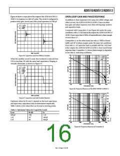
OVERLOAD RECOVERY TIME
Figure 44. Negative Overload Recovery
Overload recovery, also known as overdrive recovery, is the
time it takes the output of an amplifier to recover to its linear
region from a saturated condition. This recovery time is par-
ticularly important in applications where the amplifier must
amplify small signals in the presence of large transient voltages.
CAPACITIVE LOAD DRIVE
The AD8510/AD8512/AD8513 are unconditionally stable at all
gains in inverting and noninverting configurations. Each device
is capable of driving a capacitive load of up to 1000 pF without
oscillation in unity gain using the worst-case configuration.
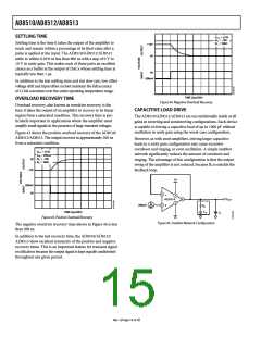
Figure 43 shows the positive overload recovery of the AD8510/
AD8512/AD8513. The output recovers in approximately 200 ns
from a saturated condition.
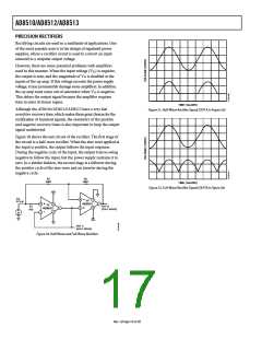
However, as with most amplifiers, driving larger capacitive
loads in a unity gain configuration may cause excessive
overshoot and ringing, or even oscillation. A simple snubber
network significantly reduces the amount of overshoot and
ringing. The advantage of this configuration is that the output
swing of the amplifier is not reduced, because RS is outside the
feedback loop.
V
V
A
R
= ±15V
= 200mV
= –100
SY
IN
0V
V
L
= 10kΩ
–15V
V+
200mV
0V
2
7
6
V
OUT
AD8510
4
3
200mV
R
S
TIME (2µs/DIV)
C
S
C
L
Figure 43. Positive Overload Recovery
V–
Figure 45. Snubber Network Configuration
The negative overdrive recovery time shown in Figure 44 is less
than 200 ns.
In addition to the fast recovery time, the AD8510/AD8512/
AD8513 show excellent symmetry of the positive and negative
recovery times. This is an important feature for transient signal
rectification because the output signal is kept equally undistorted
throughout any given period.
Rev. I | Page 14 of 20

 ROCHESTER [ Rochester Electronics ]