AD7656-1/AD7657-1/AD7658-1
Data Sheet
TABLE OF CONTENTS
Features .............................................................................................. 1
Theory of Operation ...................................................................... 20
Converter Details ....................................................................... 20
ADC Transfer Function............................................................. 21
Internal/External Reference...................................................... 21
Typical Connection Diagram ................................................... 21
Driving the Analog Inputs ........................................................ 22
Interface Options........................................................................ 22
Software Selection of ADCs...................................................... 24
Applications....................................................................................... 1
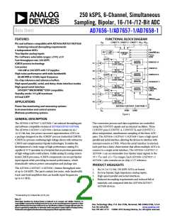
Functional Block Diagram .............................................................. 1
General Description ......................................................................... 1
Product Highlights ........................................................................... 1
Revision History ............................................................................... 2
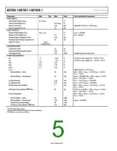
Specifications..................................................................................... 3
AD7656-1 ...................................................................................... 3
AD7657-1 ...................................................................................... 5
AD7658-1 ...................................................................................... 7
Timing Specifications .................................................................. 9
Absolute Maximum Ratings.......................................................... 10
Thermal Resistance .................................................................... 10
ESD Caution................................................................................ 10
Pin Configuration and Function Descriptions........................... 11
Typical Performance Characteristics ........................................... 14
Terminology .................................................................................... 18
H
Changing the Analog Input Range ( /S SEL = 0)................ 25
H
Changing the Analog Input Range ( /S SEL = 1)................ 25
Serial Read Operation................................................................ 25
PAR
Daisy-Chain Mode (DCEN = 1, SER/
SEL = 1)............. 27
Application Hints ........................................................................... 29
Layout .......................................................................................... 29
Power Supply Configuration..................................................... 29
Outline Dimensions....................................................................... 30
Ordering Guide .......................................................................... 30
REVISION HISTORY
3/12—Rev. C to Rev. D
Changes to Figure 28...................................................................... 22
Changes to Table 3.............................................................................7
Changes to Table 4.............................................................................9
Changes to Absolute Maximum Ratings Table .......................... 10
Changes to Pin Functions Description Table ............................. 11
Changes to Figure 9........................................................................ 14
Changes to Converter Details Section......................................... 20
Changes to Internal/External Reference Section ....................... 21
Changes to Interface Options Section ......................................... 22
Changes to Parallel Interface Section .......................................... 22
11/10—Rev. B to Rev. C
Added Power Supply Configuration Section.............................. 29
Added Figure 39.............................................................................. 29
6/10—Rev. A to Rev. B
Changes to DC Accuracy Parameter, Table 1 ............................... 3
Changes to DC Accuracy Parameter, Table 2 ............................... 5
Change to DC Accuracy Parameter, Table 3................................. 7
Added %FSR to Terminology Section ......................................... 19
Changes to Serial Interface (SER/
SEL = 1) Section .......... 25
PAR
PAR
Changes to Daisy-Chain Mode (DCEN = 1, SER/
SEL = 1) .. 27
Changes to Layout Section............................................................ 30
Updated Outline Dimension ........................................................ 31
Changes to Ordering Guide.......................................................... 31
3/09—Rev. 0 to Rev. A
Changes to Features.......................................................................... 1
Changes to Table 1............................................................................ 3
Changes to Table 2............................................................................ 5
7/08—Revision 0: Initial Version
Rev. D | Page 2 of 32

 ROCHESTER [ Rochester Electronics ]