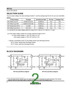
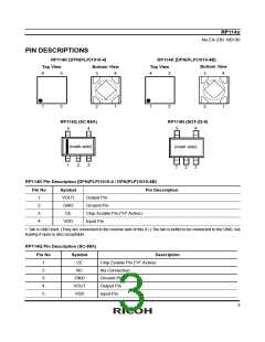
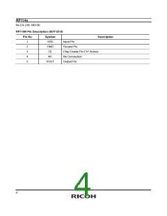
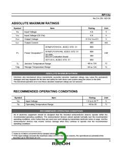
RP114x
No.EA-236-190130
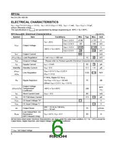
ELECTRICAL CHARACTERISTICS
VIN = VSET(1)+1.0 V (VSET > 1.5 V),VIN = 2.5 V (VSET ≤ 1.5V),IOUT = 1 mA,CIN = COUT = 1.0 µF,
unless otherwise noted.
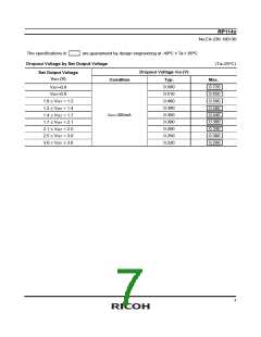
The specifications in
are guaranteed by design engineering at -40ºC ≤ Ta ≤ 85ºC.
RP114xxxxB/D Electrical Characteristics
(Ta=25C)
Symbol
Item
Conditions
VSET > 2.0 V
Min. Typ. Max.
Unit
V
0.99
-20
1.01
+20
Ta = 25C
VSET ≤ 2.0 V
VSET > 2.0 V
VSET ≤ 2.0 V
mV
V
VOUT
Output Voltage
0.97
-60
1.03
+60
-40C ≤ Ta ≤ 85C
mV
mA
mV
IOUT
VOUT/IOUT
VDIF
Output Current
Load Regulation
Dropout Voltage
Supply Current
300
1 mA ≤ IOUT ≤ 300 mA
15
40
Please refer to Product-specific Electrical Characteristics attached.
ISS
IOUT = 0 mA
VCE = 0 V
50
75
μA
μA
Istandby Standby Current
0.1
1.0
VSET + 0.5 V ≤ VIN ≤ 5.25 V
(VIN ≥ 1.4 V)
VOUT
Line Regulation
/VIN
0.02
75
0.10
%/V
dB
f=1kHz, Ripple 0.2 Vp-p,
RR
Ripple Rejection
VIN=VSET +1V, IOUT = 30 mA
(When VSET ≤ 2.0 V, VIN = 3.0 V)
Output Voltage
Temperature
Coefficient
ppm
VOUT/Ta
-40C ≤ Ta ≤ 85C
80
/C
ISC
IPD
Short Current Limit
CE Pull-down Current
CE Input Voltage “H”
CE Input Voltage “L”
VOUT = 0 V
60
mA
μA
V
0.3
0.6
0.4
VCEH
VCEL
1.0
V
BW = 10 Hz to 100 kHz,
IOUT = 30 mA
en
Output Noise
75
50
μVrms
Ω
Low Output Nch. On
Resistance
RLOW
VIN = 4.0 V, VCE = 0 V
(RP114xxxxD Only)
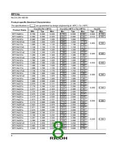
All test items listed under Electrical Characteristics are done under the pulse load condition (Tj ≈ Ta = 25ºC) except for
Output Noise, Ripple Rejection, and Output Voltage Temperature Coefficient.
(1)
V
SET
: Set Output Voltage
6

 RICOH [ RICOH ELECTRONICS DEVICES DIVISION ]