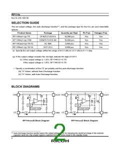
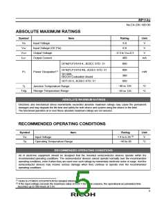
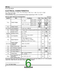
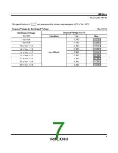
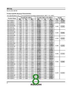
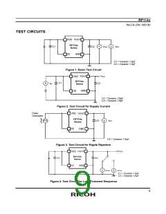
RP114x
No.EA-236-190130
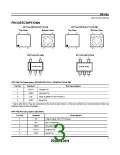
PIN DESCRIPTIONS
RP114K [DFN(PLP)1010-4]
Top View Bottom View
RP114K [DFN(PLP)1010-4B]
Bottom View
Top View
4
3
3
4
4
3
3
4
1
2
2
1
1
2
2
1
RP114Q (SC-88A)
RP114N (SOT-23-5)
5
4
5
4
(mark side)
(mark side)
1
2
3
1
2
3
RP114K Pin Description [DFN(PLP)1010-4 / DFN(PLP)1010-4B]
Pin No
Symbol
VOUT
GND
CE
Pin Description
1
2
3
4
Output Pin
Ground Pin
Chip Enable Pin ("H" Active)
Input Pin
VDD
Tab is GND level. (They are connected to the reverse side of this IC.) The tab is better to be connected to the GND, but
leaving it open is also acceptable.
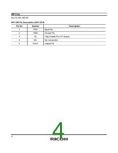
RP114Q Pin Description (SC-88A)
Pin No
Symbol
CE
Description
1
2
3
4
5
Chip Enable Pin (“H” Active)
No Connection
Ground Pin
NC
GND
VOUT
VDD
Output Pin
Input Pin
3

 RICOH [ RICOH ELECTRONICS DEVICES DIVISION ]