RP114x
No.EA-236-190130
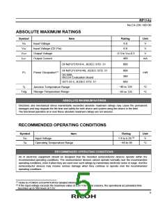
ABSOLUTE MAXIMUM RATINGS
Symbol
VIN
Item
Rating
Unit
V
Input Voltage
6.0
6.0
VCE
Input Voltage (CE Pin)
Output Voltage
Output Current
V
VOUT
IOUT
V
0.3 to VIN0.3
400
mA
DFN(PLP)1010-4, JEDEC STD. 51
DFN(PLP)1010-4B, JEDEC STD. 51
800
800
380
PD
Power Dissipation(1)
mW
SC-88A,
RICOH Evaluation Board
SOT-23-5, JEDEC STD. 51
660
40 to 125
55 to 125
C
C
Tj
Junction Temperature Range
Storage Temperature Range
Tstg
ABSOLUTE MAXIMUM RATINGS
Electronic and mechanical stress momentarily exceeded absolute maximum ratings may cause the permanent
damages and may degrade the life time and safety for both device and system using the device in the field.
The functional operation at or over these absolute maximum ratings are not assured.
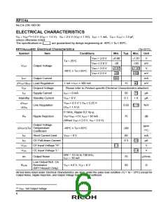
RECOMMENDED OPERATING CONDITIONS
Symbol
VIN
Item
Rating
1.4 to 5.25 (2)
−40 to 85
Unit
V
Input Voltage
Operating Temperature Range
Ta
°C
RECOMMENDED OPERATING CONDITIONS
All of electronic equipment should be designed that the mounted semiconductor devices operate within the
recommended operating conditions. The semiconductor devices cannot operate normally over the recommended
operating conditions, even if when they are used over such ratings by momentary electronic noise or surge. And the
semiconductor devices may receive serious damage when they continue to operate over the recommended
operating conditions.
(1) Refer to POWER DISSIPATION for detailed information.
(2) If the input voltage exceeds the maximum value of 5.25 V for some reasons, the operational accumulated time
becomes up to 500 hours at 5.5V.
5

 RICOH [ RICOH ELECTRONICS DEVICES DIVISION ]