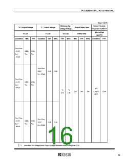
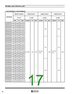
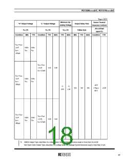
R3130N×××A/C, R3131N×××A/C
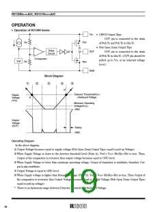
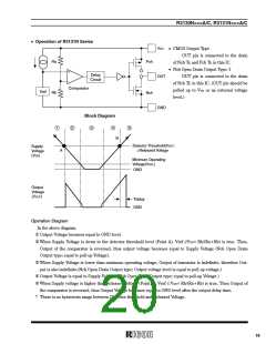
• Operation of R3131N Series
VDD
• CMOS Output Type
OUT pin is connected to the drain
of Nch Tr. and Pch Tr. in this IC.
• Nch Open Drain Output Type: I
OUT pin is connected to the drain
of Nch Tr. in this IC. (OUT pin should be
pulled up to VDD or an external voltage
level.)
Ra
Pch
Nch
+
Delay
Circuit
OUT
-
Comparator
Vref
Rb
GND
Block Diagram
1
2
3
4
5
B
Detector Threshold(VDET)
=Released Voltage
Supply
Voltage
(VDD
A
)
Minimum Operating
Voltage(VDDL
)
GND
Output
Voltage
(VOUT
)
Tdelay
GND
Operation Diagram
In the above diagram,
! Output Voltage becomes equal to GND level.
" When Supply Voltage is down to the detector threshold level (Point A), Vref ≥VDD× Rb/(Ra+Rb) is true. Then,
Output of the comparator is reversed, thus output voltage becomes equal to Supply Voltage (Nch Open Drain
Output type; equal to pull-up Voltage).
# When Supply Voltage is lower than minimum operating voltage, Output of transistor is indefinite, therefore Out-
put is also indefinite.(Nch Open Drain Output type; Output voltage level is equal to pull-up voltage.)
$ Output Voltage is equal to Supply Voltage. (Nch Open Drain Output type; equal to pull-up Voltage.)
% When Supply voltage is higher than Released Voltage (Point B), Vref ≤ VDD× Rb/(Ra+Rb) is true. Then Output of
the comparator is reversed, thus Output Voltage becomes equal to GND level after the output delay time.
* There is no hysteresis range between Detector threshold and Released Voltage.
19

 RICOH [ RICOH ELECTRONICS DEVICES DIVISION ]