R3130N×××A/C, R3131N×××A/C
OPERATION
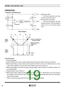
• Operation of R3130N Series
VDD
• CMOS Output Type
OUT pin is connected to the drain
Ra
Pch
Nch
of Nch Tr. and Pch Tr. in this IC.
• Nch Open Drain Output Type
OUT pin is connected to the drain
of Nch Tr. in this IC. (OUT pin should be
pulled up to VDD or an external voltage
level.)
+
Delay
Circuit
OUT
-
Comparator
Vref
Rb
GND
Block Diagram
1
2
3
4
5
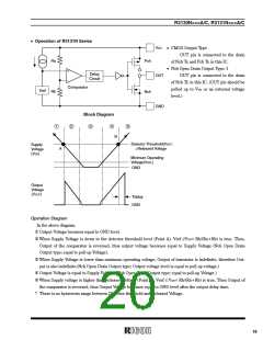
B
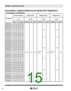
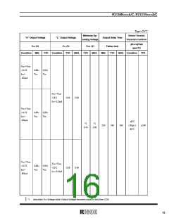
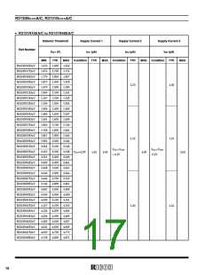
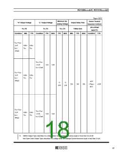
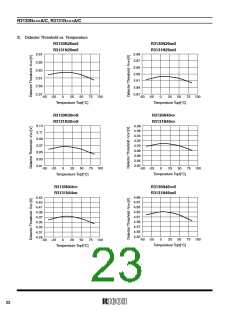
Detector Threshold(VDET)
=Released Voltage
Supply
Voltage
(VDD
A
)
Minimum Operating
Voltage(VDDL
)
GND
Output
Voltage
(OUT)
Tdelay
GND
Operating Diagram
In the above diagram,
Output Voltage becomes equal to supply voltage (Nch Open Drain Output Type; equal to pull-up Voltage).
!
" When Supply Voltage is down to the detector threshold level (Point A), Vref ≥ VDD× Rb/(Ra+Rb) is true. Then,
Output of the comparator is reversed, thus output voltage becomes equal to GND level.
# When Supply Voltage is lower than minimum operating voltage, Output of transistor is indefinite, therefore Out-
put is also indefinite.
$ Output Voltage is equal to GND level.
% When Supply voltage is higher than Released Voltage (Point B), Vref ≤ VDD× Rb/(Ra+Rb) is true. Then Output of
the comparator is reversed, thus Output Voltage becomes equal to Supply Voltage (Nch Open Drain Output Type;
equal to pull-up voltage).
* There is no hysteresis range between Detector threshold and Released Voltage.
18

 RICOH [ RICOH ELECTRONICS DEVICES DIVISION ]