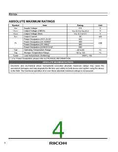
R3112x
ABSOLUTE MAXIMUM RATINGS
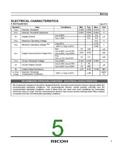
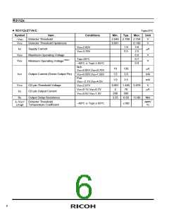
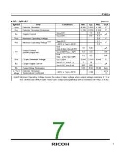
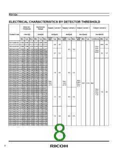
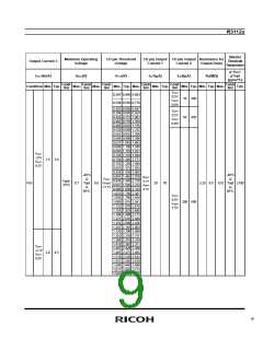
Symbol
VDD
Item
Rating
Unit
V
Supply Voltage
6.5
VSS−0.3 to VDD+0.3
VSS−0.3 to 6.5
20
VOUT1
VOUT2
IOUT
Output Voltage (CMOS)
V
Output Voltage (Nch)
V
Output Current
mA
Power Dissipation (SOT-23-5)*
Power Dissipation (SC-82AB)*
Power Dissipation (SC-88A)*
Power Dissipation (SON1612-6)*
Operating Temperature Range
Storage Temperature Range
Lead temperature (Soldering)
420
380
PD
mW
380
500
Topt
Tstg
−40 to 85
−55 to 125
°C
°C
Tsolder
260°C, 10s
* ) For Power Dissipation, please refer to PACKAGE INFORMATION.
ABSOLUTE MAXIMUM RATINGS
Electronic and mechanical stress momentarily exceeded absolute maximum ratings may cause the
permanent damages and may degrade the life time and safety for both device and system using the device
in the field. The functional operation at or over these absolute maximum ratings is not assured.
4

 RICOH [ RICOH ELECTRONICS DEVICES DIVISION ]