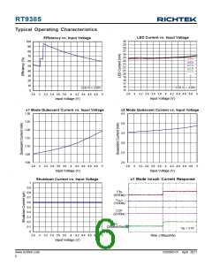
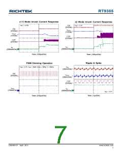
RT9385
the RT9385, The maximum junction temperature is 125°C.
The junction to ambient thermal resistance θJA is layout
dependent. For WQFN-16L 2x3 package, the thermal
resistance θJA is 90°C/W on the standard JEDEC 51-7
four layers thermal test board. The maximum power
dissipation at TA = 25°C can be calculated by following
formula :
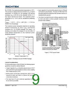
` Input capacitor (CIN) should be placed close to VINand
connected to ground plane. The trace of VINin the PCB
should be placed far away from the sensitive devices or
shielded by the ground.
` The traces running from pins to flying capacitor should
be short and wide to reduce parasitic resistance and
prevent noise radiation.
PD(MAX) = (125°C − 25°C) / (90°C/W) = 1.111W for
WQFN-16L 2x3 package
All the traces of LED pins running from
chip to LEDs should be wide and short to
reduce the parasitic connection resistance.
The maximum power dissipation depends on operating
ambient temperature for fixed TJ(MAX) and thermal
resistance θJA. For RT9385 package, the Figure 1 of
derating curve allows the designer to see the effect of
rising ambient temperature on the maximum power
dissipation allowed.
The trace from CF pin
to external capacitance
should be as short as
possible.
Output capacitor
(C
) should
OUT
16 15 14
be placed close
to VOUT and
connected to
ground plane to
reduce noise
coupling from
charge pump to
LEDs.
1
2
3
4
5
13
12
11
10
9
LED3
LED4
LED5
VOUT
PGND
AGND
CF
1.2
GND
VIN
Four Layers PCB
Battery
1.1
EN
1.0
Input capacitor
C2P
17
(C ) should be
IN
0.9
6
7
8
WQFN-16L 2x3
placed close to VIN
and connected to
ground plane. The
trace of VIN in the
0.8
0.7
0.6
0.5
0.4
0.3
0.2
0.1
0.0
GND
GND
PCB should be
placed far away
The traces running from pins to flying capacitor from the sensitive
should be short and wide to reduce parasitic
resistance and prevent noise radiation.
devices or shielded
by the ground.
Figure 2. PCB Layout Guide
0
25
50
75
100
125
Ambient Temperature (°C)
Figure 1.Derating Curve for RT9385 Package
Layout Considerations
For best performance of the RT9385, the following layout
guidelines should be strictly followed :
` Output Capacitor (COUT) should be placed close to VOUT
and connected to ground plane to reduce noise coupling
from charge pump to LEDs.
` All the traces of LED pins running from chip to LED's
should be wide and short to reduce the parasitic
connection resistance.
` The trace from CF pin to external capacitance should
be as short as possible.
DS9385-01 April 2011
www.richtek.com
9

 RICHTEK [ RICHTEK TECHNOLOGY CORPORATION ]