RT9385
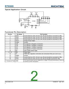
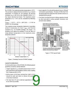
Typical Application Circuit
C
FLY2
C
FLY1
1µF
1µF
8
7
9
6
C1P C1N C2P C2N
14,11
VIN
15
16
PWM Input
LED1
LED2
LED3
LED4
LED5
C
1µF
IN
10
4
EN
RT9385
1
2
3
VOUT
C
12
OUT
CF
1µF
AGND
13
PGND
C
CF
5
0.1µF
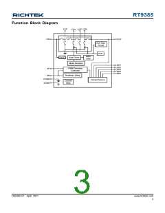
Functional Pin Description
Pin No.
Pin Name
LED3
Pin Function
1
2
Current Sink for LED3. (If not in use, this pin should be connected to VIN)
Current Sink for LED4. (If not in use, this pin should be connected to VIN)
Current Sink for LED5. (If not in use, this pin should be connected to VIN)
Charge Pump Output.
LED4
LED5
VOUT
PGND
C2N
C1N
C1P
3
4
5
Ground.
6
Fly Capacitor 2 Negative Connection.
7
Fly Capacitor 1 Negative Connection.
8
Fly Capacitor 1 Positive Connection.
9
C2P
Fly Capacitor 2 Positive Connection.
10
11, 14
12
13
15
16
EN
Chip Enable (Active High).
VIN
Power Input.
CF
PWM Filter Capacitor Connection, No Connection if this pin is not in use.
Ground.
AGND
LED1
LED2
Current Sink for LED1. (If not in use, this pin should be connected to VIN)
Current Sink for LED2. (If not in use, this pin should connected to VIN)
The exposed pad must be soldered to a large PCB and connected to GND for
maximum power dissipation.
17 (Exposed Pad) GND
www.richtek.com
2
DS9385-01 April 2011

 RICHTEK [ RICHTEK TECHNOLOGY CORPORATION ]