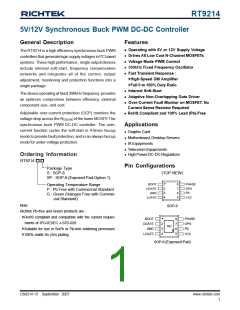
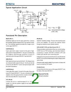
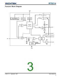
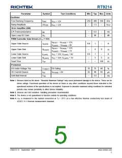
RT9214
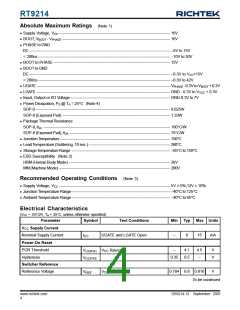
Parameter
Symbol
Test Conditions
Min
Typ Max Units
Oscillator
Free Running Frequency
Ramp Amplitude
250
--
300
1.5
350
--
kHz
f
V
V
= 12V
OSC
CC
ΔV
V
P-P
= 12V
OSC
CC
Error Amplifier (GM)
E/A Transconductance
Open Loop DC Gain
--
--
0.2
90
--
--
ms
dB
g
m
A
O
PWM Controller Gate Drivers (VCC = 12V)
V
V
V
V
− V
= 12V,
= 6V
BOOT
PHASE
Upper Gate Source
0.6
--
1
4
--
8
A
I
UGATE
− V
UGATE
PHASE
PHASE
− V
= 12V,
= 1V
BOOT
Upper Gate Sink
R
Ω
UGATE
− V
UGATE
PHASE
Lower Gate Source
Lower Gate Sink
Dead Time
0.6
--
1
3
--
5
A
Ω
I
V
= 12V, V
= 6V
= 1V
LGATE
CC
CC
LGATE
R
V
= 12V, V
LGATE
LGATE
--
--
100
ns
T
DT
Protection
FB Under-Voltage Trip
OC Current Source
Soft-Start Interval
FB Falling
= 0V
70
35
--
75
40
80
45
--
%
Δ
FBUVT
SS
I
V
μA
ms
OC
PHASE
3.5
T
Note 1. Stresses listed as the above "Absolute Maximum Ratings" may cause permanent damage to the device. These are for
stress ratings. Functional operation of the device at these or any other conditions beyond those indicated in the
operational sections of the specifications is not implied. Exposure to absolute maximum rating conditions for extended
periods may remain possibility to affect device reliability.
Note 2. Devices are ESD sensitive. Handling precaution recommended.
Note 3. The device is not guaranteed to function outside its operating conditions.
Note 4. θJA is measured in the natural convection at TA = 25°C on a low effective thermal conductivity test board of
JEDEC 51-3 thermal measurement standard.
www.richtek.com
5
DS9214-13 September 2007

 RICHTEK [ RICHTEK TECHNOLOGY CORPORATION ]